-48V Hot Swap Solution For Telecom Line Cards Assures Immunity To Input Voltage Transients
摘要
Step-by-step instructions are provided for selection of the appropriate external components with the MAX5900/MAX5901 -48V hot-swap controller to design a hot swap solution for Telecom line cards. The solution provides inrush current limit control, immunity to input voltage transients and short circuit protection.
Hot-swap controllers provide the basic functions of limiting inrush current, reducing high-current stress on connectors, and eliminating system power glitches as cards are plugged into a hot backplane, but no protection is provided for large input-voltage transients. This application note describes how to select components peripheral to the hot-swap controller to assure proper operation and circuit survival in the face of 36V input transients and output short circuits.
Figure 1 illustrates a typical telecom-system power-distribution configuration. The front end provides EMI filtering, transient-voltage suppression, and connection to input-voltage sources. Conditioned power is then routed to the backplane sockets where line cards are installed. However, the act of battery substitution can cause up to a 36V step on the -48V bus.
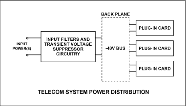
Figure 1. Typical telecom system power distribution configuration.
The hot-swap controller itself provides the normal functions of limiting inrush current charging of the bulk capacitor on the plug-in card during hot swapping, preventing glitches on the system back plane at card installation, and reducing high-current stresses on the connectors. Many hot-swap controllers also contain circuit-breaker functions that actuate in the presence of preset overload currents. For the telecom application where large step input-voltage transients may occur, the circuit-breaker function can disconnect the card when the large input transient charges the on-card bulk capacitor, so circuit-breaker functions cannot be safely used.
Figure 2 shows a simple telecom hot-swap controller circuit using the MAX5900NN to provide normal hot-swap protection without an internal circuit breaker; it satisfies system requirements in the presence of positive and negative input-voltage transients and protects the back-plane during output short circuits. Continuous operation in the presence of high-current bulk-capacitor charge during large input-voltage steps, as well as backplane protection from short-circuits, can be achieved when MOSFET and on-card fuse characteristics are selected to match system requirements.
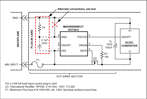
Figure 2. The MAX5900NNEUT hot-swap application circuit for telecom system.
Theory of Operation
Card Plug-In
As the card is plugged into the backplane during normal hot swapping operation, the controller holds power switch Q1 in the OFF state for 300ms, allowing time for the card to be firmly in place and connector-contact bounce to settle before power is applied to the load. Following the start-up delay, the controller gradually turns Q1 ON, limiting the inrush current charging CL by controlling the output voltage rise rate (δVOUT/δt) sensed at the DRAIN pin. Meanwhile, the active-low PGOOD status output signal holds the following DC/DC converter OFF to prevent added load current during the inrush phase. Thus, the total inrush current drawn by the plug-in card is only the conditioned inrush current charging the load capacitor. The δVOUT/δt is limited to 10V/ms, so the inrush current is limited to
![]()
Positive (Magnitude) Input Step Voltage
A positive input-voltage step can occur when lightning strikes, when power is restored after a brown out, or during battery swap when a fresh battery is plugged into a back plane running on a nearly-depleted battery. Once the startup phase is complete, the hot-swap controller without circuit-breaker function no longer controls inrush currents that occur due to input-voltage transients. The battery swap condition will be most likely to cause the greatest bulk-capacitor charging current because a common battery-swap test condition is a 36V step, abruptly increasing VIN from -36V to -72V. At this time, Q1 should pass the capacitor-charging current without sustaining damage, yet the fuse should not blow. This is easy to say, but it takes some knowledge of fuse trip time vs. current and MOSFET transient thermal properties to make a proper selection of components. See the Selecting Components section for detailed information on how to achieve this goal. Short-pulse transients due to lightening disturbances as attenuated by the backplane input filter and transient suppressor circuitry and are expected to be less severe in this regard than the battery-swap test.
Negative (Magnitude) Input Step Voltage
The MAX5900 device will operate properly in the presense of negative transients so long as two supply voltage conditions are met. The input voltage must not drop below its 9V minimum operating range, and the input voltage must not drop below the programmed UVLO trigger point for more than 20msec. Two kinds of transients should be considered. One is caused when a card with inadequate hot-swap control is hot plugged into the back plane; another is caused by lightning-induced transients.
- The card-plug-in negative transient will be of but a few hundred millivolts or a few volts at most as the backplane impedance is expected to support cold-plug connecting with little voltage sag. Controller operation will be unaffected by this type of transient so long as the two supply-voltage conditions listed above are met.
- A lightening-induced transient can be positive, negative, or oscillatory in nature with the waveform lasting from several to a few tens of microseconds depending upon the effectiveness of the backplane input filter and transient suppressor circuitry. Associated narrow negative transients could extend below the minimum 9V operating range of the controller to cause momentary dropouts. If this condition is expected, the modifications to the circuit of Figure 2 inside the dashed lines would suffice for short-pulse (100msec) dropouts to zero volts. Conditions for survival of Q1 and the fuse in the presence of large negative pulses are similar to those for large positive pulses. See the Selecting Components section for further information
A second consideration is that the negative input-voltage transient causes the load capacitor to discharge to the backplane through Q1's RDS(ON). The back-charging current creates a voltage drop across Q1, possibly bringing the VEE terminal voltage to more than 0.3V above DRAIN to forward bias the internal ESD diode connected between source and drain. If circuit-trace resistance, load-capacitor ESR1, and capacitor and circuit ESL2 are negligible, almost the entire negative peak voltage of a steep transient would appear across Q1 as the transient attempts to discharge the bulk capacitor. Even if parasitic circuit resistance and inductance are non-negligible, it requires little additional negative-voltage step magnitude to forward bias the ESD diode. Placing R3 in the circuit limits current into the DRAIN pin to protect the MAX5900 during this transient. The recommended value of R1 is 1kΩ to 10kΩ.
Output Short Circuit
When the output is short circuited, full input voltage is applied between Q1 drain and source with current limited by Q1's ID(ON). As ID(ON) will be at least several tens of amperes, the high power dissipation in Q1 can be sustained only briefly before it fails in a shorted condition. In the meantime, fast-blow fuse F1 has time to heat and blow open as soon as Q1 fails short. F1 permanently disconnects the faulty plug-in card from the system, preventing a catastrophic system failure. When an already short-circuited (defective) card is hot-plugged into the backplane, short-circuit current is limited in the same way with the fuse providing system protection. As a shorted card is likely to be considered as expendable, Q1 failure is of little importance. If Q1 failure is unacceptable, Q1 must be selected to allow survival during the time it takes the fuse to blow. See the Selecting Components section for further information.
Selecting Components
Both the fuse and Q1 should survive unharmed during positive or negative step transient testing, yet the fuse (and possibly Q1) should blow quickly under short-circuit conditions. Initially, the MOSFET and fuse selections are made to allow stable and uninterrupted operation under normal operating load conditions. Then consideration must be given to the 36V positive voltage step test condition or a large negative pulse step, and finally to the short-circuit condition. The selection process can be demonstrated using the example of Figure 2 for 2.5A full-load operation.
- Select the fuse with some safety factor for continuous 2.5A operation, but with consideration given to an additional safety factor for positive step transients. One would use at least a 3A fuse. A 4A fuse is tentatively selected.
- Select Q1 to have insignificant full-load voltage drop VDS(ON) and/or an acceptable and sustainable power loss PD. Voltage drop appears across the drain-to-source resistance of Q1 plus an additional drop across the connector and circuit trace resistances. Assume that the circuit traces are appropriately sized for minimum drop, and consider Q1's ID(ON), rDS(ON), and PD. ID(ON) must certainly be greater than full-load current IFL, but that requirement will be easily met when rDS(ON) is selected. In this example a PD = 1W is selected as reasonable. Then

A Fairchild Semiconductor IRF530 160mΩ MOSFET with ID(ON) ≈ 50A meets the selection criteria. For lower power loss, select a MOSFET with lower rDS(ON) such as the International Rectifier IRF530 90mΩ MOSFET. Both exhibit ID(ON) ≈ 50A. - Calculate capacitor charging current under a 36V step-transient condition. Initially, the step transient presents the peak transient voltage across the series sum of [RDS(ON) + fuse resistance + CL's ESR] plus whatever exists in the transient source impedance, and ESL of traces, capacitors and filters. ESL, particularly, acts to slow steeply rising waveforms. The worst-case conditions exist when we consider only the known RDS(ON) (100mΩ–300mΩ depending upon junction temperature), RFUSE (35mΩ typical from manufacturer's data sheet), and capacitor ESR (≈ 40mΩ for 100µF low ESR varities).

but charging current is initially limited by Q1's ID(ON) ≈ 50mA until the MOSFET emerges from saturation and operation enters the resistive region, when the current decays exponentially to zero. - Determine the current pulse width, the voltage across the MOSFET, and the peak transient power in the MOSFET. The applied 36V transient will be distributed across RDS(ON), RFUSE, and capacitor ESR.

Simulation is helpful here (see Figure 3) although it is acceptable for our purpose to assume a triangular power pulse with the calculated width. Inspection of Figure 3 will show that our simple calculation closely approximates the simulated conditions. Power and pulse width of interest is ½PD(PK) for ΔT.
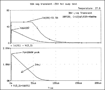
Figure 3. Positive line transient waveforms.
- Determine MOSFET temperature rise during the transient. We want the MOSFET to survive this power pulse without overheating. So it is now time inspect the transient thermal resistance curve from the Fairchild IRF530 data sheet as reproduced in Figure 4. Entering the curve at 75µsec
(7.5 x 10⁻⁵) on the horizontal axis, and rising vertically to intercept the solid (single pulse) line, we read the transient thermal resistance on the vertical axis to be ΘJC = 0.05°C/W. We calculate junction

This is easily within limits as junction temperature is allowed to reach 175°C. The MOSFET will surely survive this power pulse.
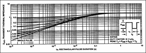
Figure 4. Transient thermal resistance, Fairchild IRF530 (courtesy: Fairchild Semiconductor).
- Select a fuse that will survive this < 100µsec transient without blowing. To do this, a curve of time vs. current is required for the selected fuse. This curve can be obtained from the fuse manufacturer, and is reproduced in Figure 5. The left curve boundary indicates that any value to left of the curve will not blow the fuse. The right curve boundary indicates that any value to right of the curve must blow the fuse. The curves become straight lines near and below the horizontal axis, so may be extrapolated to 100µsec to find the current multiplier for minimum and maximum time limits at amperage. Extrapolating the curves to 100µs indicates that the fuse will not blow at 22 times rated current (88A) at 100µsec. We also see that at least 7 times the rated current (28A) is required for fuse blow in 1msec, while blow is guaranteed at 10 times rated current (40A) in 10msec. Extrapolating the curves to 100µs indicates that the fuse will blow at 12 times rated current (48A) in 8msec, or will blow at 40X (160A) in 1msec. The selected 4A fuse is a suitable choice as it allows safe operation on 36V transients, yet will blow in < 8msec at ID(ON)-limited 50A short-circuit conditions, or will blow in ≤ 1msec if Q1 shorts during short-circuit, so we may select a 4A (no blow at 88A/100µsec) fuse, although we have yet to verify performance under short-circuit conditions.
- Determine the current and MOSFET power dissipation under short-circuit conditions. If a short circuit is placed on the output of the hot-swap circuit at CL, Q1 current is determined by ID(ON)
≈ 50A as before. The short circuit places the entire supply voltage across the MOSFET in series with the fuse resistance. Neglecting the fuse resistance provides a worst-case calculation of
PD(SC) = 48V × 50A = 2400W. We already know from Step 6 that the fuse must blow at 48A in 8msec. Therefore, we are curious to know if Q1 will survive 2400W for 8msec. Entering the curve of Figure 4 at 8msec, we find a single-pulse thermal resistance of 0.59°C/W. A new calculation indicates a junction temperature rise of 0.59°C/W × 2400W = 1440°C. Even if the fuse should blow at 2msec (midway between the min and max curves) junction temperature rise would be 851°C. This is well above the melting point of aluminum die metalization, and the MOSFET would be destroyed in under 2msec. Q1 will fail shorted and the fuse will blow.
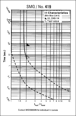
Figure 5. Fuse current-time characteristics (courtesy Wickmann).
Summary
The chosen circuit is exceptionally simple, allows reliable operation under normal operating and test conditions, yet fuse protection will interrupt a short-circuited board in two milliseconds or less. The importance of making an informed selection of fuse and pass transistor in simple hot-swap circuits such as this is demonstrated.
Notes
- Effective series resistance
- Effective series inductance


