48V Hot Swap Circuit Blocks Reverse Battery Voltage
Hot Swap controllers guard against inrush current and short circuits, but reverse battery installation is another matter. In central office applications, OR-ing diodes block reversed input voltages. In systems with a single power source OR-ing diodes become unnecessary; although a single diode could be retained for reverse conditions, its forward drop loss is a significant penalty.
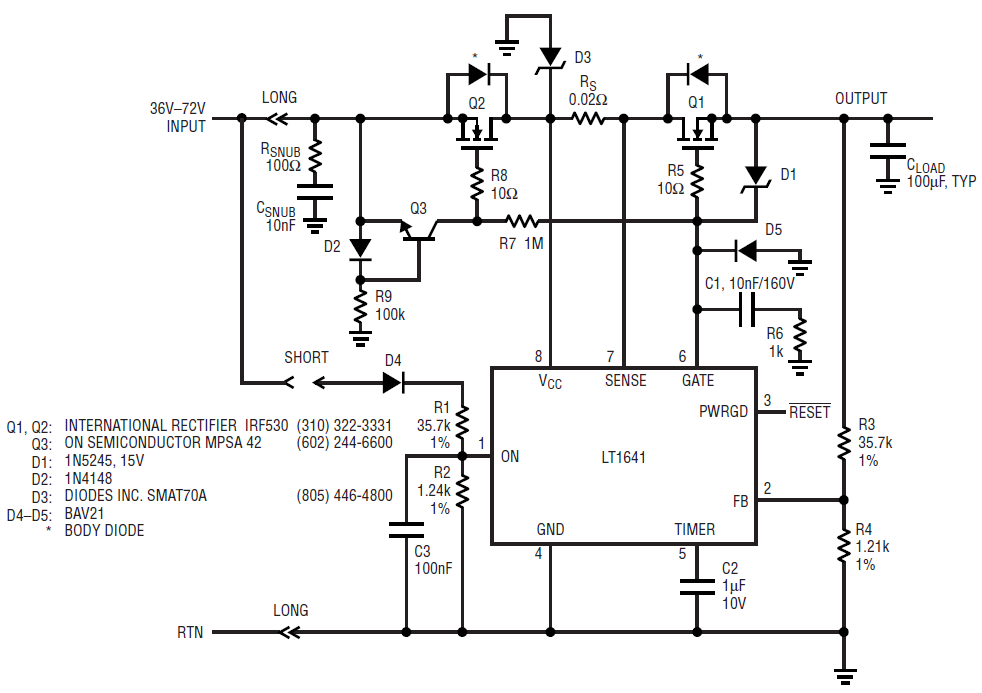
The circuit shown in Figure 1 eliminates the loss associated with a blocking diode. The LT1641 and Q1 handle familiar hot swap chores of undervoltage lockout, inrush control, short circuit protection and system reset, while Q2 and Q3 handle reverse input situations.

Figure 1. Reverse-battery protected LT1641 48V Hot Swap circuit.
Under positive input conditions, Q2’s body diode is forward biased and power reaches the LT1641 and Q1, allowing them to function in the normal manner. When the LT1641 is commanded to turn on, GATE (pin 6) and R7 slowly charge C1, thereby limiting the inrush current to CLOAD. The LT1641 drives both Q1 and Q2 fully into enhancement mode, minimizing losses and eliminating the drop in Q2’s body diode.
Q3 is included as part of the circuitry that blocks reverse inputs, yet it must “get out of the way” when positive inputs are present. With a positive input, Q3’s emitter is pulled up, dragging along its base via D2. Since the base is slightly negative with respect to the emitter, Q3 is off. A small current flows through resistor R9 to ground, but this is of no consequence. If the LT1641 is in the off state, GATE pulls low. Current flows from the forward-biased collector-base junction of Q3 to the LT1641’s GATE pin, but is limited by R7. When the LT1641 turns on, GATE pulls up above the input supply and the collector-base junction of Q3 becomes reverse-biased. Q3 is off, so no collector current flows and the LT1641’s GATE output is not loaded by Q3.
If a reverse input polarity is applied, Q3 goes to work and ensures that Q2 is held off. Negative inputs pull the emitter of Q3 below ground. Q3 turns on, biased by R9, and the collector effectively shorts Q2’s gate and source. With Q2 in the off state, no current can flow into RS, the LT1641 or Q1. The circuit can take up to –100V in this condition. Of course, some leakage current does flow in Q2; this is absorbed by D3.
This circuit can handle instantaneous steps from zero to ±75V. As shown, short circuit protection limits the output to 2.5A. Q1, Q2, and RS can be scaled to handle loads in excess of 1kW.


