2-Phase Synchronous Buck Controller Delivers Maximum Features in Minimum Footprint
2-Phase Synchronous Buck Controller Delivers Maximum Features in Minimum Footprint
2007-10-01
Introduction
The LTC3850 is a feature-rich dual channel synchronous step-down switching regulator available in a 4mm × 4mm QFN package. It is designed to meet today’s high performance power application needs. With constant frequency peak current mode control for clean operation over a broad range of duty cycles, the LTC3850 is a response to customer requests for a cost-effective solution that balances ease of use, efficiency, precision and performance.
Familiar Features, and Some New Ones
The LTC3850’s two channels run out of phase, which reduces the input RMS current ripple and thus the input capacitance requirement. Switching frequency can be adjusted from 250kHz to 780kHz, either set with a voltage on the FREQ/PLLFLTR pin, or synchronized to a signal into the MODE/PLLIN pin using a phase-locked loop. During high frequency operation, the LTC3850 can operate normally at low duty cycles due to its short top switch minimum on-time. For example, a 20V to 1.5V converter operating at 700kHz requires a minimum on-time of less than

The LTC3850 can cycle its strong top gate drivers in just 90ns, making this low duty cycle application a reality.
At heavy loads, the LTC3850 operates in constant frequency PWM mode. At light loads, it can switch in any of three modes (Figure 1). Burst Mode operation switches in pulse trains of one to several cycles, with the output capacitors supplying energy during intervening sleep periods. This provides the highest possible light load efficiency. Forced continuous mode offers PWM operation from no load to full load, providing the lowest possible output voltage ripple. Pulse skipping mode operates at a constant frequency, but always turns off the synchronous switch before inductor current is allowed to reverse. This method reduces light load ripple compared to Burst Mode operation and improves light load efficiency compared to forced continuous mode.
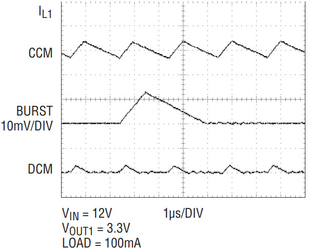
Figure 1. Three modes of operation. Continuous mode features predictable, constant frequency operation. Burst Mode® operation has the best light-load efficiency, with somewhat higher output ripple. Pulse skip mode is a compromise between the other two.
Tracking provides a predictable way of slewing the output voltages up or down. Tracking generally holds the feedback voltage to the lesser of the internal reference voltage or the voltage on a TRACK pin. The LTC3850 goes farther by combining track and soft start functions in a single pin for each channel and by tailoring the mode of switching operation to the state of the TK/SS pins.
When TK/SS is ramping up from ground to 0.8V, either from its 1.3µA internal current source or by tracking another supply, the channel remains in pulse skipping mode until the TK/SS voltage reaches 0.64V. This prevents the regulator from sinking current from the output while it is at 80% or less of the target voltage. When TK/SS ramps up from 0.64V to 0.74V, the channel operates in forced continuous mode to ensure that the power good indicator (PGOOD) makes just one transition from low to high when the output comes into regulation (within ±7.5% of the precision 0.8V reference). Once 0.74V (the undervoltage threshold) is reached, the regulator transitions to the mode of switching operation programmed on the MODE/PLLIN pin. When TK/SS is descending from 0.8V, forced continuous mode takes over when VTK/SS and VFB ramp from 0.74V down to 0.1V, allowing the LTC3850 to pull down the output at the programmed slew rate. Once TK/SS ramps down to 0.1V, the channel begins operating in pulse skipping mode. Switching stops when TK/SS is less than the feedback voltage.
Each channel also features a separate RUN pin with a precision 1.2V turn-on threshold. When the LTC3850’s own current source is used to charge the soft-start capacitor, bringing a channel’s RUN pin high causes its soft-start capacitor to begin charging within about 80µs. As an alternative, either RUN pin can remain high while TK/SS is held low, which keeps the internal 5V regulator enabled as a standby supply. This feature can be used to power a wake-up circuit which controls the state of both TK/SS pins.
Two Ways to Sense Current
The LTC3850 features a fully differential comparator to sense current through the inductor. The SENSE+ and SENSE– pins can be connected to a sense resistor in series with the inductor, or to an RC network in parallel with the inductor for energy efficient sensing across the inductor’s DC resistance (DCR sensing). Using 1% tolerance sense resistors offers an accurate current limit, but incurs I2R losses in the resistors. DCR sensing prevents this power loss, but uses a sense element with a typical built in error of 5%-10%. The LTC3850 can use either method, with a choice of three pin-selectable current limits.
When an output sees a short circuit, the LTC3850 protects the input supply and power components by limiting peak current cycle by cycle. The main MOSFET turns off when the inductor’s peak current sense threshold (VSENSE(MAX)/RSENSE) is reached. VSENSE(MAX) can be set to 30mV, 50mV, or 75mV, for a wide range of output current levels. Duty cycle has little effect on this current limit (Figure 2). For load currents greater than the programmed maximum but less than a hard short, the LTC3850 gracefully folds back the top MOSFET’s on-time, reducing the output voltage.
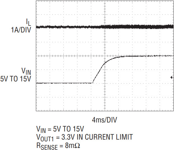
Figure 2. The LTC3850 is a peak current mode controller. As such, it uses a compensating ramp on the inductor upslope to ensure stability at duty cycles greater than 50%. Alone, the ramp would cause current limit to drop at high duty cycles, but the LTC3850 uses a patent-pending scheme to prevent this behavior. Here, the LTC3850 is operating in current limit, and peak current is well-controlled when duty cycle swings from 66% to 22%.
The LTC3850 also protects against undervoltage input and overvoltage output voltages. The RUN pins can be referenced to a voltage divider from VIN, so that their precision thresholds control the state of the outputs. If the output voltage is more than 7.5% above its target, the bottom MOSFET can remain on until regulation is recovered. If the LTC3850 is allowed to operate with a main input voltage approaching the programmed output voltage, its duty cycle can be as high as 97%.
Dual Output, 5A Regulator with DCR Sensing
Figure 3 shows the schematic for a 500kHz, 2-output regulator requiring no sense resistors. By using the inductor’s DC resistance as the current sense element, the application dissipates as little power as possible—at full load current, efficiency is well above 90%, as Figure 4 shows.
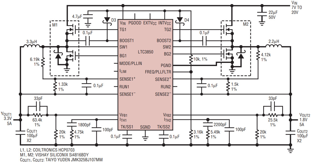
Figure 3. Schematic for a 2-channel, 5A/500kHz regulator with DCR sensing.
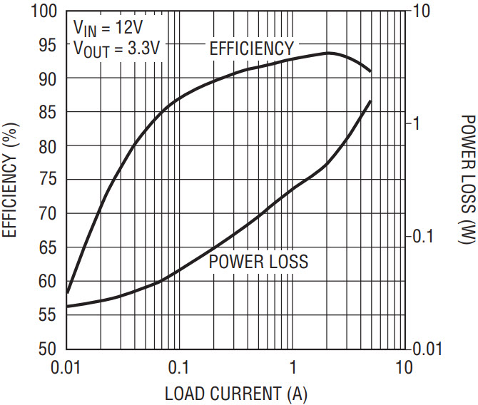
Figure 4. Efficiency and power loss for Figure 3, Channel 1.
Dual Output, 15A Regulator with Sense Resistors
Figure 5 shows the schematic for an efficient 400kHz, 2-output regulator. Figure 6 shows that this circuit’s core occupies less than a square inch on a 2-layer board. Peak inductor current is limited to 25A by the maximum current sense threshold looking across the sense resistor (50mV / 2mΩ). Taking inductor ripple current into account, the output current limit is around 20A for each channel. Higher load current will cause the LTC3850 to protect the power stage using current foldback.
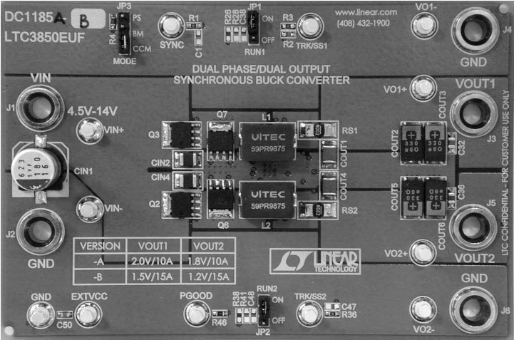
a. Top view.
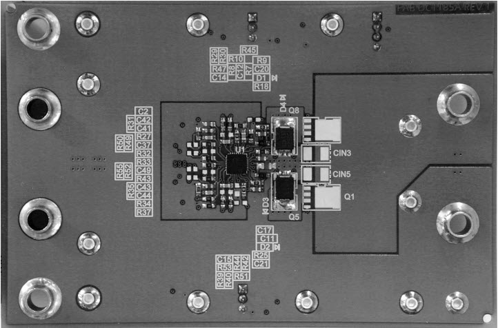
b. Bottom view.
Figure 6. The circuit of Figure 5 can be laid out inside a square inch on a two-layer board.
Conclusion
The LTC3850 delivers copious features in small packages. Available in 4mm × 4mm 28-pin QFN (0.4mm lead pitch), 4mm × 5mm 28-pin QFN (0.5mm lead pitch), or 28-pin narrow SSOP, it can run at high efficiency using DCR sensing and Burst Mode operation. Tracking, strong on-chip drivers, multiphase operation, and external sync capability fill out its menu of features. Ideal for notebook computers, PDAs, handheld terminals and automotive electronics, the LTC3850 delivers multiphase power to mission critical applications.


