摘要
As TFT-LCD displays become more prevalent in automobiles, the size and resolution become an even greater concern for the automotive industry. In this design solution, we highlight how the MAX25520 2-channel TFT-LCD power supply addresses several of the common design challenges that display modules face. Primarily, it provides higher current for bigger displays. Additionally, we show how the IC's high level of integration and synchronous boost converter work together to lower BOM cost and ease of implementation.
Introduction
The modern car contains numerous displays ranging from implementation in instrument clusters to center-stack touchscreens (Figure 1), rear-seat entertainment, and more. The vast automotive display market is dominated by TFT-LCD technologies while OLEDs may play a significant role in the future. In this highly competitive scenario, TFT-LCDs have high current and precision needs.

Figure 1. Modern car center-stack touchscreen.
Typical TFT-LCD Display System
Figure 2 illustrates the simplified block diagram of a typical automotive display. The display receives power through multiple rails and the video signal through the gigabit multimedia serial link (GMSL), converting serial LVDS data to a parallel interface in RGB format. A high voltage buck converter provides the main 5V or 3.3V rail feeding the rest of the low-voltage circuits, while the high-voltage LDO provides the always-on power to the MCU. As the size and resolution of the TFT-LCD increase, a separate TFT bias is needed to supply the source drivers.
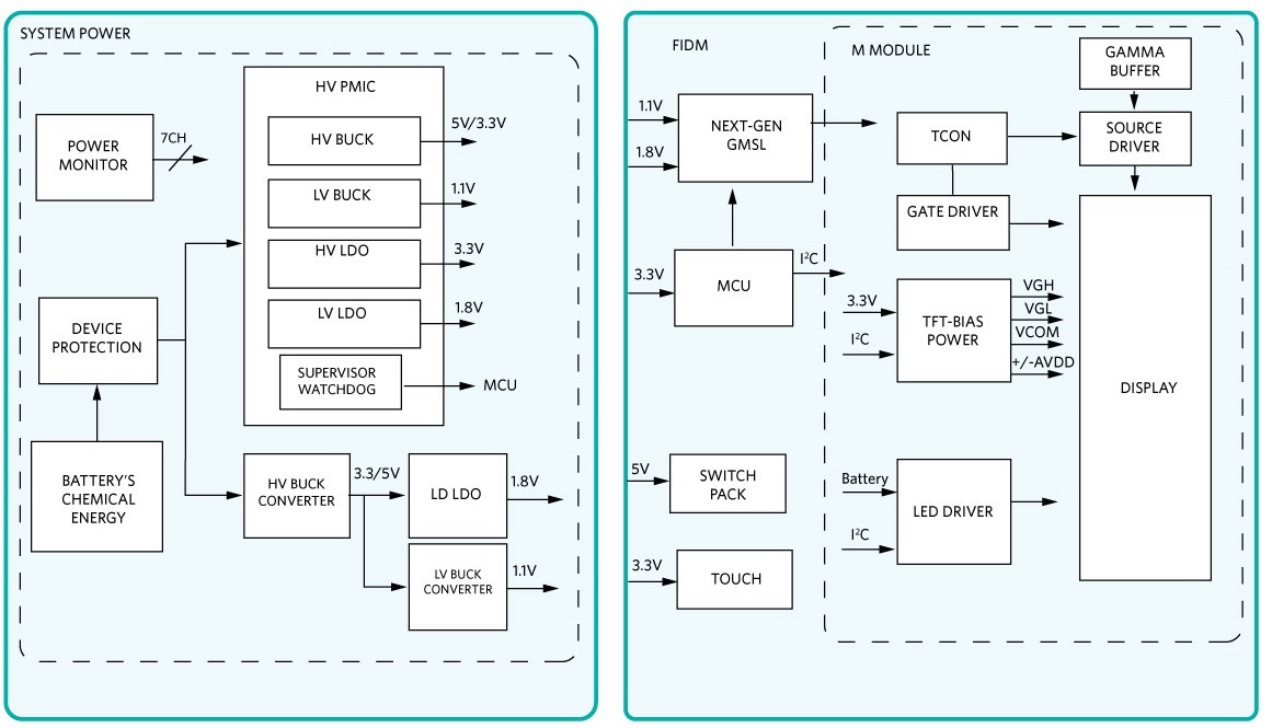
Figure 2. TFT-LCD display simple block diagram.
TFT-Bias Sub-System
Figure 3 illustrates the detailed TFT-bias block diagram circuitry when utilizing a TFT-bias device such as the MAX25520. The MAX25520 addresses several of the common design challenges that display modules face. Primarily, it provides higher current for bigger displays. Additionally, the high level of integration and synchronous boost converter work together to lower the BOM cost and ease of implementation. The MAX25520 continues to rise above the competition by offering 2.1MHz switching and robust spread spectrum to reduce electromagnetic interference. Finally, MAX25520 (Figure 4) supplies both positive and negative AVDD source voltages. Bipolar AVDD source voltage supplies are often associated with higher-performance panels such as low-temperature polysilicon (LTPS) panels.
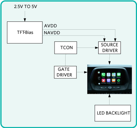
Figure 3. TFT-bias detailed block diagram.
Design Example
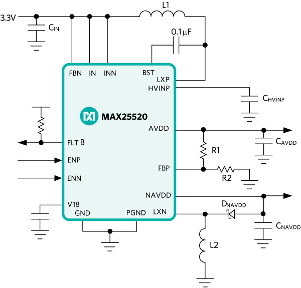
Figure 4. MAX25520 application circuit.
| Design Parameter | Value |
| Input Voltage Range | 3.3V±5% |
| Boost Output Voltage/Current | 6V/200mA |
| Inverter Output Voltage/Current | -6V/-200mA |
| Switching Frequency | 2.1MHz |
| Reference | Value | Description |
| CIN | 2x10mF | Capacitor, Ceramic, 6V, X7R |
| L1 | 2.2mH | Inductor, +20%, 2.3A |
| L2 | 4.7mH | Inductor, +20%, 2.3A |
| CHVINP | 10mF | Capacitor, Ceramic, 10V, X7R |
| CAVDD | 1mF | Capacitor, Ceramic, 10V, X7R |
| CNAVDD | 10mF | Capacitor, Ceramic, 10V, X7R |
| R1 | 68kO | Resistor, 1%, 0.1W |
| R2 | 12kO | Resistor, 1%, 0.1W |
| DNAVDD | Schottky | Diode, 2.25A peak |
Detailed Design Procedure
Selecting the appropriate component types and values ensures optimum device operation and allows the attainment of maximum efficiency and lowest niose operation. The following sections describe how to make critical design component selections according to the application circuit example shown in Figure 4.
Output Voltage Selection
The MAX25520 includes a current-mode boost converter with output switch that can generate an output up to +10.5V (+12V for MAX25520ATEC) and delivering up to 200mA. The boost converter's regulation voltage (AVDD) is set by the resistor-divider between AVDD and GND with the midpoint connected to FBP. FBP is regulated to a nominal voltage of 0.9V.
Select the resistor values using the following equation:

R1 is the resistor connected from AVDD to FBP, R2 is the resistor connected from FBP to ground, and VAVDD is the desired output voltage. In this design, use R1 = 68kO and R2 = 12kO.
The inverting current-mode buck-boost converter (NAVDD) can generate an output down to 10.5V ( 12V for MAX25520ATEC), delivering up to 200mA, and is internally compensated.
As in this design, when FBN is connected to IN/INN, the NAVDD voltage mirrors the regulated voltage on AVDD.
If a voltage other than -VAVDD is required, connect a resistor-divider from V18 to NAVDD with its midpoint connected to FBN. Select the resistor values using the following equation:

R4 is the resistor connected between FBN and NAVDD, R3 is the resistor from V18 to FBN, and VNAVDD is the desired output voltage. Use a value greater than 4.7kO for R3.
Boost Converter Inductor Selection
Three key inductor parameters must be specified for operation with the device: Inductance value (L), inductor saturation current (ISAT), and DC resistance (RDC).
To determine the inductance value, first select the ratio of inductor peak-to-peak ripple current to average output current (LIR). A good compromise between size and loss is to use a value between 0.3 and 0.6 for the LIR ratio. However, the AC characteristics of the inductor core material and the ratio of the inductive resistance to other power path resistances can influence the selection of LIR. If thin high-resistance inductors are used, as is common for LCD-panel applications, the best LIR may lie between 0.5 and 1.0. Further LIR selection can be optimized depending on operating regions and load variations. After selecting LIR, the inductance value is determined as follows:
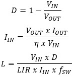
where VIN is the input voltage, VOUT is the positive output voltage, IOUT is the output current, IIN is the calculated average boost input current, ? is the efficiency of the boost converter, D is the duty cycle, and fSW is the switching frequency. The inductor's saturation rating must exceed the maximum current limit of 2.25A.
Using a LIR of 0.7 and an efficiency of 90% the calculated inductor value is 2.5mH. Converting this value to the nearest standard value, use a value of 2.2mH for this design.
Inverting Regulator Inductor Selection
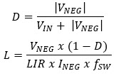
where VIN is the input voltage, VNEG is the negative output voltage, INEG is the output current, LIR is the desired inductor ripple ratio, and fSW is the switching frequency.
The inductor's saturation current rating must exceed the maximum current limit of 2.25A.
Using a LIR of 0.9, the calculated inductor value is 5.6mH. We use a value of 4.7mH for this design.
Input Capacitor Selection
The function of the input capacitor is to maintain a steady input voltage to the IC. Sufficient input capacitance must be used to avoid input voltage drop when the AVDD and NAVDD converters require high input currents, especially during device startup. If the IN voltage drops below 2.57V, the device will likely reset. Therefore, input capacitance must prevent this from happening. The total value of capacitance depends on the expected transients and the series resistance in the IN connection. An input capacitance consisting of two parallel 10mF ceramic capacitors is a good starting value for this design. Adding a lower-value (0.1mF) ceramic capacitor between the input and ground can also help to absorb high-frequency currents.
Output Capacitor Selection
The primary criterion for selecting the output filter capacitor is low effective series resistance (ESR). The product of the peak inductor current and the output filter capacitor's ESR determine the amplitude of the high-frequency ripple seen on the output voltage.
On the boost output, HVINP, use a ceramic capacitor of at least 22mF at 420kHz and 10mF at 2.1MHz to ensure stability. Output ripple can be further reduced by increasing the output capacitance while ensuring a low ESR.
To avoid a large drop on HVINP when AVDD is enabled, the capacitance on the HVINP node should be at least 3 times larger than that on AVDD.
In this design, we select a 10mF capacitor for use on the HVINP pin while we place 1mF on AVDD.
The primary criteria for selecting the NAVDD output filter capacitor are low ESR and capacitance value as this capacitor provides the load current when the internal switch is on. The voltage ripple on the NAVDD output has two components: ripple due to ESR and ripple due to bulk capacitance.
A 10mF ceramic capacitor is needed on the NAVDD output to ensure stability. Increasing this outut capacitance reduces output ripple further. In this design, the chosen 10mF capacitor yields less than 10mVP-P output ripple.
NAVDD External Diode Selection
For the NAVDD external diode, the peak current rating should be at least equal to the LXN current limit (2.25A). The diode breakdown-voltage rating should exceed the sum of the maximum VINN and the absolute value of VNAVDD. A Schottky diode improves the overall efficiency of the converter.
Conclusion
TFT-LCDs dominate the automotive display market and are entering a very competitive phase as new technology emerges. Displays greater than 10 inches need a TFT-bias to resolve the added power needs stemming from increased size and resolution. In this MAX25520 design solution, we provided a detailed step-by-step design guide showing how to use the MAX25520 and provide a balance of a simple yet robust solution.
Learn More:
MAX25520 2-Channel TFT-LCD Power Supply.


