12-Bit, 1.25Msps ADC with 8-Channel Programmable MUX Offers Incredible Versatility
12-Bit, 1.25Msps ADC with 8-Channel Programmable MUX Offers Incredible Versatility
by
Dave Thomas
2001-12-01
Close Your Eyes, Make a Wish
Think about everything you have ever wanted from a multiplexed ADC: plenty of channels with a fast per-channel throughput rate; single-ended or differential inputs, or both; unipolar and bipolar input spans; multiple input ranges. Take all of that, throw in the ability to reconfigure on the fly, automatically scan through all of the channels or program and run a sequence of up to sixteen addresses and configurations and you are only beginning to understand the power of the new LTC1851. If you are tired of adapting your inputs to fit your ADC, Analog Devices offers an ADC that can adapt to your inputs.
The LTC1851 has an 8-channel input multiplexer, a programmable sample-and-hold and an internal reference. The 12-bit, 1.25Msps ADC runs off of a single 5V supply, drawing only 25mW. The part has NAP and SLEEP shutdown modes and good DC and AC specs. Figure 1 is a simplified diagram of the signal path of the LTC1851, showing the individual blocks and control signals. The LTC1851 uses six configuration control bits (DIFF, A2, A1, A0, UNI/BIP and PGA) and three operational modes to provide unprecedented flexibility to fit your application.
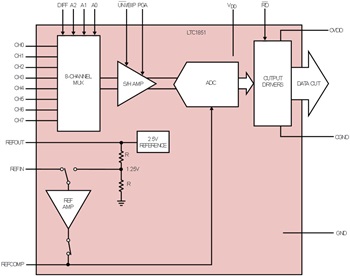
Figure 1. Simplified block diagram shows programmable MUX, sample-and-hold and 3-pin reference interface.
Input Multiplexer Handles Single-Ended or Differential Inputs
What kind of signals do you need to convert—single-ended? No problem. The LTC1851 can be configured for eight single-ended inputs, each relative to a common pin (COM). The COM pin can be connected to ground or used to offset the negative input. Differential? Again, no problem. The eight channels of the LTC1851 can be configured as four differential pairs (Channel 0 and Channel 1, Channel 2 and Channel 3 and so on). Choosing between the two modes is as easy as connecting the DIFF pin to ground or to the supply. In addition, the DIFF bit can be changed between conversions, even when the LTC1851 is running at the full conversion rate, effectively reconfiguring the MUX with every conversion. Figure 2 illustrates the possibilities. With DIFF tied low you get eight single-ended inputs. With DIFF tied high you get four differential pairs. Changing the DIFF bit with the MUX Address for each conversion can provide any desired combination of single-ended and differential inputs.
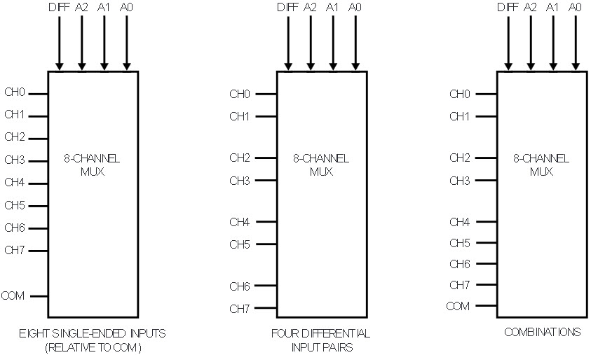
Figure 2. Input multiplexer handles single-ended or differential inputs or combinations.
The MUX Address Inputs (A2, A1, A0) select the “positive” input. In the single-ended case, the COM pin will always be the “negative” input. In the differential case, the “negative” input will be the other input of the pair. Note that this method allows either input of a differential pair to be the “positive” input, allowing the user to choose the polarity. Table 1 summarizes the MUX Address Input selection. Regardless of the configuration of the Input MUX, the inputs to the ADC are always truly differential, meaning that both inputs are sampled simultaneously. Any noise or signal that is common to both inputs will be rejected.
| MUX Address | Single-Ended Channel Selection | |||||||||||
| DIFF | A2 | A1 | A0 | CH0 | CH1 | CH2 | CH3 | CH4 | CH5 | CH6 | CH7 | COM |
| 0 | 0 | 0 | 0 | + | – | |||||||
| 0 | 0 | 0 | 1 | + | – | |||||||
| 0 | 0 | 1 | 0 | + | – | |||||||
| 0 | 0 | 1 | 1 | + | – | |||||||
| 0 | 1 | 0 | 0 | + | – | |||||||
| 0 | 1 | 0 | 1 | + | – | |||||||
| 0 | 1 | 1 | 0 | + | – | |||||||
| 0 | 1 | 1 | 1 | + | – | |||||||
| MUX Address | Differential Channel Selection | |||||||||||
| DIFF | A2 | A1 | A0 | CH0 | CH1 | CH2 | CH3 | CH4 | CH5 | CH6 | CH7 | COM |
| 1 | 0 | 0 | 0 | + | – | |||||||
| 1 | 0 | 0 | 1 | – | + | |||||||
| 1 | 0 | 1 | 0 | + | – | |||||||
| 1 | 0 | 1 | 1 | – | + | |||||||
| 1 | 1 | 0 | 0 | + | – | |||||||
| 1 | 1 | 0 | 1 | – | + | |||||||
| 1 | 1 | 1 | 0 | + | – | |||||||
| 1 | 1 | 1 | 1 | – | + | |||||||
Programmable Sample-and-Hold and Reference Provide Multiple Input Ranges
The flexibility of the LTC1851 is also apparent in its wide selection of input ranges. The sample-and-hold gives you the option of unipolar or bipolar inputs and a choice of two gains, and is completely programmable. The reference, although not programmable in the strictest sense, offers three pin-strappable options using the internal reference and two options for using an external reference. Together, the sample-and-hold and reference provide a choice of ten different input ranges using the internal reference (unipolar ranges of 0V–1.024V, 0V–1.25V, 0V–2.048V, 0V–2.5V and 0V–4.096V, and bipolar ranges of ±0.512V, ±0.625V, ±1.024V, ±1.25V and ±2.048V) and virtually unlimited ranges using an external reference. The input range is set by programming the sample-and-hold to determine the input span relative to the full-scale reference (REFCOMP) and then configuring the reference to determine REFCOMP.
Programming the Sample-and-Hold for Unipolar/Bipolar Mode and Gain
The sample-and-hold of the LTC1851 lets you choose either a unipolar or bipolar input and a gain of one or two. When UNI/BIP is low, a unipolar input range of 0 – SPAN is selected. When UNI/BIP is high, a bipolar input range of ±SPAN/2 is selected. It should be noted that in bipolar mode the inputs must always be between the supply rails and are not allowed to be above VDD or below ground. The “negative” input should be connected to a common mode voltage (typically midsupply or midreference) and the “positive” input swings ±SPAN/2 around the common mode voltage. The PGA bit selects the gain of the sample-and-hold and determines how the input SPAN relates to REFCOMP. If PGA is held high, the SPAN will be equal to REFCOMP (gain of one). If PGA is held low, the SPAN will be equal to REFCOMP/2 (gain of two). With two bits of control the user can select one of four input ranges relative to REFCOMP: 0–REFCOMP, ± REFCOMP/2, 0–REFCOMP/2, and ±REFCOMP/4. Table 2 illustrates the input range options of the LTC1851. It is important to remember that, just like the input MUX, the state of the sample-and-hold can be changed between conversions while the LTC1851 is running at the full conversion rate of 1.25Msps.
| REFCOMP = 4.096V | ||||
| PGA = 0 | PGA = 1 | PGA = 0 | PGA = 1 | |
| UNI/BIP = 0 | 0V–REFCOMP/2 | 0V–REFCOMP | 0V–2.048V | 0V–4.096V |
| UNI/BIP = 1 | ±REFCOMP/4 | ±REFCOMP/2 | ±1.024V | ±2.048V |
Setting the Full-Scale Reference
The last piece of the puzzle concerning the input range is to set the full-scale reference, which is set by the voltage that appears on the REFCOMP pin. Again, the LTC1851 gives the user a number of choices. The LTC1851 offers three pin-strappable options for REFCOMP as well as two additional options for using an external reference or DAC. The onboard reference of the LTC1851 consists of a 2.5V reference and a reference buffer with an accurately trimmed gain of 1.6384 (see Figure 1). The REFOUT pin is the output of the 2.5V reference, the REFIN pin is the input to the reference buffer and also acts as a control pin to select the reference buffer mode and the REFCOMP pin is the output of the reference buffer.
If REFIN is driven with a voltage of 1V to 2.6V, the reference buffer will produce a voltage of 1.6384 • REFIN on the REFCOMP pin. REFIN can be connected to REFOUT to produce a REFCOMP voltage of 4.096V using the internal reference or REFIN can be driven by an external reference or DAC. If REFIN is held high, the reference buffer will be disabled and REFCOMP can be driven directly. In this mode, REFCOMP can be connected to REFOUT to produce a 2.5V range using the internal reference or REFCOMP can be driven by an external reference or DAC. Finally, if REFIN is held low, the input to the reference buffer is switched to a voltage representing REFOUT/2. This produces a voltage on REFCOMP of 2.048V using the internal reference. Figure 3 summarizes the five reference modes.
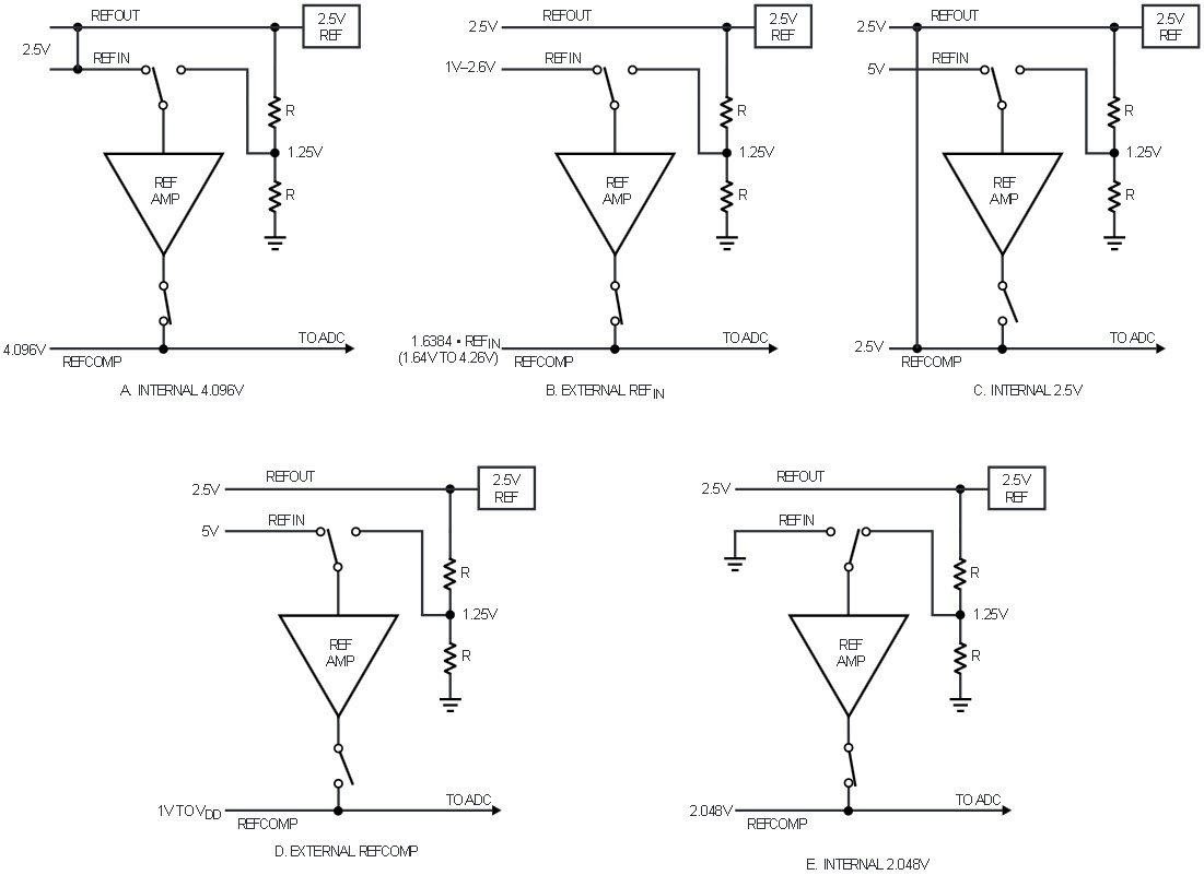
Figure 3. Reference options: A. internal reference using reference amplifier; B. external reference using reference amplifier; C. internal reference bypassing reference amplifier; D. external reference bypassing reference amplifier; E. one-half of internal reference using reference amplifier.
The LTC1851’s internal reference, reference buffer and the gain and full scale of the input are all trimmed independently. This method ensures accuracy regardless of the reference configuration.
Output Word Automatically Includes Address and Data Format Switches
At the end of every conversion, the LTC1851 outputs a 16-bit parallel word that includes the 12-bit data word (D11–D0) and the 4-bit MUX Address (DIFF out, A2 out, A1 out, A0 out). This provides the user with the conversion result as well as the configuration (single-ended or differential) and address of the inputs that were sampled to obtain it (see Figure 4). The 12-bit data word automatically changes format depending on the status of the UNI/BIP bit when the conversion starts. If the UNI/BIP bit was low at the start of the conversion, indicating a unipolar input, the format of the 12-bit data word will be straight binary. If the UNI/BIP bit was high, indicating a bipolar input, the format of the 12-bit data word will be two’s complement. During a normal conversion cycle RD acts as an output enable control. The sixteen outputs are enabled when RD is low and are high impedance when RD is high. All sixteen outputs and BUSY run off of the separate OVDD and OGND supplies to make it easy to interface to 3V logic. Table 3 summarizes the output data format.
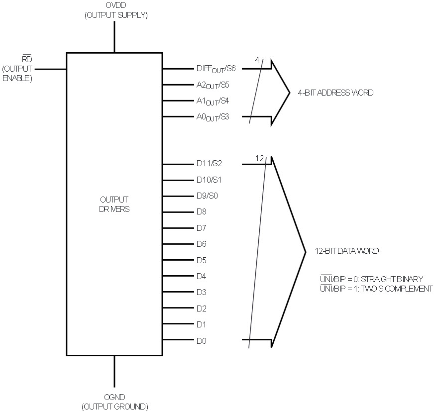
Figure 4. Output word automatically includes address and data-format switches.
| Unipolar Mode (UNI/BIP = 0) | |||
| Output Code | Input Voltage | ||
| REFCOMP = 4.096V | |||
| PGA = 0 VFS = 2.048V |
PGA = 1 VFS = 4.096V |
||
| 1111 1111 1111 | VFS – 1LSB | 2.0475V | 4.095V |
| 1111 1111 1110 | VFS – 2LSB | 2.047V | 4.094V |
| |
|||
| 1000 0000 0001 | (VFS/2) + 1LSB | 1.0245V | 2.049V |
| 1000 0000 0000 | VFS/2 | 1.024V | 2.048V |
| 0111 1111 1111 | (VFS/2) - 1LSB | 1.0235V | 2.047V |
| 0111 1111 1110 | (VFS/2) - 2LSB | 1.023V | 2.046V |
| |
|||
| 0000 0000 0001 | 1LSB | 0.0005V | 0.001V |
| 0000 0000 0000 | 0 | 0V | 0V |
| Bipolar Mode (UNI/BIP = 1) | |||
| Output Code | Input Voltage | ||
| REFCOMP = 4.096V | |||
| PGA = 0 VFS = 1.024V |
PGA = 1 VFS = 2.048V |
||
| 0111 1111 1111 | VFS – 1LSB | 1.0235V | 2.047V |
| 0111 1111 1110 | VFS – 2LSB | 1.023V | 2.046V |
| |
|||
| 0000 0000 0001 | 1LSB | 0.0005V | 0.001V |
| 0000 0000 0000 | 0 | 0V | 0V |
| 1111 1111 1111 | –1LSB | –0.0005V | –0.001V |
| 1111 1111 1110 | –2LSB | –0.001V | –0.002V |
| |
|||
| 1000 0000 0001 | –VFS + 1LSB | –1.0235V | –2.047V |
| 1000 0000 0000 | –VFS | –1.024V | –2.048V |
Manual, Semiautomatic and Fully Automatic Operation
The best thing about the flexibility of the LTC1851 is that you can choose how much of it you want to use. It is easy to use in the simplest applications but has enough power to handle almost anything you can throw at it. The LTC1851 accomplishes this by offering three distinct operating modes that correspond roughly to manual, semiautomatic and automatic.
Manually Set It and Forget It, or Reconfigure It for Every Conversion
Sometimes a MUX doesn’t need to be fancy and superprogrammable, it just needs to be a MUX. In Direct Address Mode (see Figure 5) it is very easy to set the LTC1851 up as an 8 × 1 or 4 × 2 MUX with a single input range for all channels. The DIFF, UNI/BIP and PGA pins can be tied high or low so all that is needed is to send an address on the A2, A1, and A0 input pins to select the channel to convert. The rising edge of WR can be used to latch the data on these six pins or WR can be tied low to leave the pins always enabled (in which case the falling edge of CONVST will latch the data until the end of the conversion). If your application is a little more demanding, you can still take advantage of the programmability of the LTC1851 in Direct Address Mode by driving the DIFF, UNI/BIP and PGA pins in addition to the Address Input pins. In fact, you can change all six Configuration Control bits (DIFF, A2, A1, A0, UNI/BIP and PGA) between conversions at the full conversion rate of 1.25Msps. Again, WR functions as an input enable pin, enabling the six configuration control pins when low and latching on the rising edge.
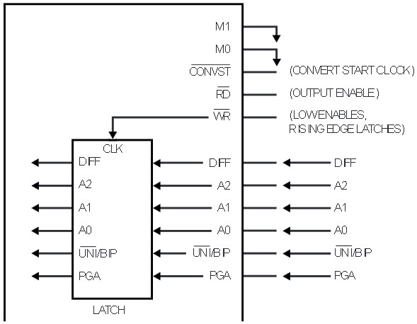
Figure 5. Direct address mode.
Scan All Channels Semiautomatically
It is very common to have several sensors connected to a MUX and an ADC that repeatedly converts each channel in succession. The MUX address must be updated for each conversion normally requiring a processor or an external counter to keep track of and increment the address. The LTC1851 Scan Mode (see Figure 6) solves this problem by handling the addressing so that all that is needed is a stream of CONVST pulses. The DIFF, UNI/BIP and PGA pins function the same way they do in the Direct Address mode (enabled when WR is low and latched on the rising edge of WR) but the Address pins are ignored. Instead, the LTC1851 uses an internal counter to provide the MUX Address. It starts at address 000 (reset to 000 on either edge of M0) and steps through each channel. The counter is smart enough to adjust the step size depending on the state of the DIFF pin. If the DIFF pin is low, it will step the address by one through eight single-ended channels (CH0–COM, CH1–COM, CH2–COM, CH3–COM, … CH7–COM, repeat). The throughput rate for each channel is 1.25Msps/8 or 156.25kHz. If the DIFF pin is high, it will step the address by two to scan through the four differential pairs (CH0–CH1, CH2–CH3, CH4–CH5, CH6–CH7, repeat). In this case, the throughput rate for each differential pair is 1.25Msps/4 or 312.5kHz. It is also possible to vary the internal counter step size by changing the state of the DIFF pin between conversions. For example, if the A0 output is connected to DIFF, the LTC1851 will sequentially convert the following pattern of four single-ended inputs and two differential pairs: CH0–COM, CH1–COM, CH2–CH3, CH4–COM, CH5–COM, CH6–CH7, repeat. Remember that WR must be held or clocked low for changes on the DIFF pin to be recognized. An added bonus is that the 4-bit MUX address is available with each conversion result as part of the 16-bit data output word. This provides a foolproof way to synchronize a conversion result with the input channel (or channels) it represents.
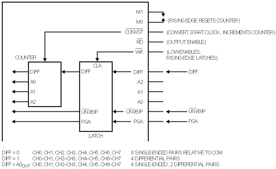
Figure 6. Scan mode.
Fully Automatic Programmable Sequencer Solves the Toughest Problems
Now let’s look at two problems where the power of the LTC1851 really begins to shine. First, let’s imagine the following set of inputs that we would like to scan continuously: Input A has a range of 0V–4.096V, input B has a range of 0V–2.048V, input C has a range of ±2.048V that swings around 2.5V, input D has a range of ±1.024V and is truly differential with a common mode of 2V (each input swings between 1.488V and 2.512V) and input E has a range of 1V–3.048V. We could use the Direct Address Mode but it’s going to require that we send an address and configuration for each conversion, over and over again. We could use the Scan Mode to handle the addressing but it doesn’t fit any of the obvious scan patterns and we’re still going to have to use processing power to drive the UNI/BIP and PGA pins to switch the sample-and-hold.
The second problem is extremely common. Let’s say we have eight single-ended channels to convert but one of the channels needs to be sampled much faster (for example, 500kHz) than the other seven (for example, 50kHz). Again, we could use the Direct Address Mode but we have to send the same pattern of addresses over and over again, or we could use the Scan Mode but that divides the throughput evenly among the eight channels, limiting each channel to 156.25kHz—not fast enough for the fast channel.
The answer to both of these problems is the LTC1851 Sequencer Mode. In this mode, all control of the six configuration control bits is relinquished to a programmable sequencer. The sequencer has a memory of sixteen locations that allows the user to program a repeating pattern of up to sixteen steps, where each step is an independent MUX address and configuration. This is useful for configuring the MUX for any combination of single-ended and/or differential inputs, unipolar and/or bipolar inputs and two gains. In the first problem, the LTC1851 can be easily programmed to run a five-step sequence to read all five of these sensors sequentially and automatically. The first step reads Channel 0, single-ended, unipolar, with a gain of one to get a 0V–4.096V range for input A. The second step switches to Channel 1 and a gain of two to get a 0V–2.048V range for input B. The third step switches back to a gain of one, switches the MUX to differential, switches the sample-and-hold to bipolar and converts Channel 2-Channel 3 with the input C connected to Channel 2 and Channel 3 connected to 2.5V. The fourth step switches to a gain of two using Channels 4 and 5 as a differential pair (input D). The fifth and last step uses Channels 6 and 7 differential, unipolar, gain of two with the input E connected to Channel 6 and Channel 7 connected to 1V. The LTC1851 then cycles through these addresses and configurations, each with a throughput of 1.25Msps/5 or 250kHz, with nothing more than a series of CONVST pulses.
The second problem is just as easily solved by the sequencer’s ability to program an arbitrary pattern of addresses, allowing the user to allocate the throughput per channel as needed. A throughput of 625kHz on Channel 0 and throughputs of 89.28kHz on Channels 1–7 can easily be achieved by programming a pattern of CH0, CH1, CH0, CH2, CH0, CH3, CH0, CH4, CH0, CH5, CH0, CH6, CH0, CH7, repeat. Again, the LTC1851 will run this pattern with just a series of CONVST pulses and will provide channel identity with each conversion result.
Writing to the Sequencer
How is the sequencer used? First, it is necessary to store the sequence of conversions the LTC1851 is to perform. To write to the sequencer, the RD pin must be held high, the M0 pin taken low and WR taken low (see Figure 7). The first falling edge of WR enables the Configuration Control inputs (DIFF, A2, A1, A0, UNI/BIP and PGA). The rising edge of WR latches the current state of those pins into the sequencer location 0000 and advances the pointer to the next location. Subsequent WR low pulses will continue to write up to sixteen locations. After the last desired location is written, M0 should be taken high and the sequence is ready to run beginning at location 0000.
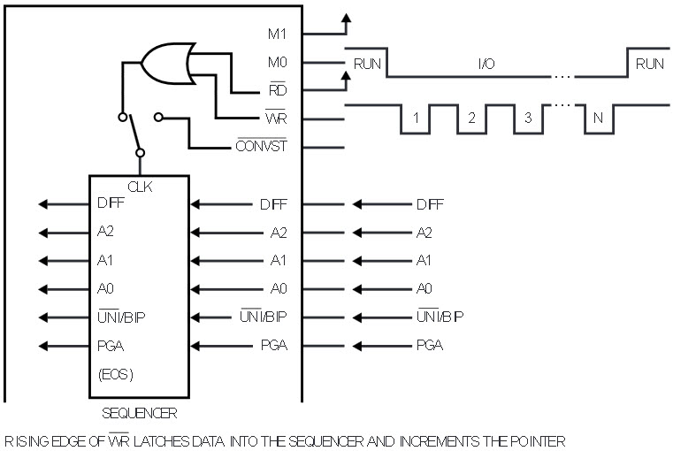
Figure 7. Writing to the sequencer.
Reading the Sequencer
In many applications, it is important to confirm the integrity of the programmed sequence before beginning conversions or before resuming conversions after a potentially disruptive event. The LTC1851 allows the user to read back the entire contents of the sequencer to confirm the program before running. WR must be held high, M0 taken low and RD taken low (see Figure 8). The first falling edge of RD will output the contents of the first sequencer location and enable the seven Status Word output pins (S6–S0). The next rising edge of RD will return the output pins to a high impedance state and increment the pointer to the next sequencer location. Subsequent RD low pulses will read through all sixteen locations and then return to location 0000. The last location in the current sequence will be indicated by a logic 1 on the S0 pin.
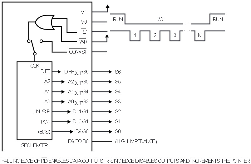
Figure 8. Reading the sequencer.
Running the Sequencer
Now the program is stored and checked and ready to run. The M0 pin must be returned high, which will reset the pointer to location 0000 (see Figure 9). The LTC1851 will then begin acquiring the input signal using the configuration stored in the first sequencer memory location. The first falling edge of CONVST will sample the inputs, begin a conversion and increment the pointer so that when the conversion is finished, the LTC1851 will begin acquiring the next input using the configuration stored in sequencer memory location 0001. This continues until the last programmed location is reached, after which the sequencer will return to location 0000. The program stored in the sequencer memory is retained as long as power is continuously applied to the part. This allows the user to jump between any of the three modes (Direct Address, Scan or Sequencer) or into and out of the NAP or SLEEP shutdown modes and retain the stored program. The user can run a programmed sequence, interrupt and take direct control of the MUX or shut the converter down and then return to the programmed sequence. Any edge of M1 or M0 will reset the counter and/or pointer so that Scan Mode always starts at MUX address 000 and the sequencer always starts at location 0000.
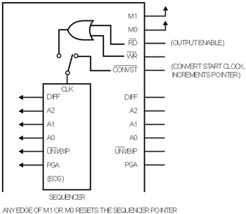
Figure 9. Running the sequencer.
Conclusion
The LTC1851 has everything you’ve ever wanted from a Multiplexed ADC. It has a programmable input MUX and sample-and-hold that can handle single-ended, differential, unipolar or bipolar inputs. It has a flexible reference that offers three internal ranges and two options for using an external reference. The ADC is a low power, high performance 12-bit, 1.25Msps converter. The three operational modes make it easy to use in the simplest applications but powerful enough to solve your toughest problems. Stop adapting your inputs to the ADC and start using an ADC designed to adapt itself to your inputs and your application.


