


概览
设计资源
描述
MAXREFDES1169是基于MAX17681的高效、iso-buck DC-DC电源模块,可接受17V至32V输入电压范围,通过原边反馈调整输出电压。参考设计提供四路输出:±15V@75mA和±7.5V@75mA,稳压精度±10%。该款iso-buck隔离电源模块采用10引脚 (3mm × 2mm) TDFN封装的MAX17681设计。MAXREFDES1169的引脚间距符合分布式电源开放标准联盟(DOSA)的DC/DC模块电源开放标准。提供两种变压器选项,一种来自于Wurth;另一种来自于中国变压器厂家HanRun,方便用户选型。参考设计提供1500V电气隔离。
优势和特点
- ±15V@75mA和±7.5V@75mA输出,输出电压纹波180mV
- 17V至32V输入电压范围
- EN/UVLO输入
- 200kHz开关频率
- 89%峰值效率
- 过流保护
- 无光耦设计
- 输出功率高达3.4W
- 热保护
- 经过验证的PCB布板
详情
The MAX17681/MAX17681A is a high-voltage, highefficiency, iso-buck DC-DC converter designed to provide isolated power up to 5W. The device operates over a wide 4.5V to 42V input and uses primary-side feedback to regulate the output voltage. The MAX17681/MAX17681A uses peak-current-mode control. Low-resistance, on-chip MOSFETs ensure high efficiency at full load while simplifying the PCB layout. The MAX17681/MAX17681A devices generate a well-regulated primary side voltage, which is then scaled by a suitable transformer turns ratio to derive isolated secondary output rails. While both the MAX17681 and MAX17681A support primary side overcurrent protection, the MAX17681A is an enhanced design that also supports robust secondary-side overcurrent protection. The MAX17681/MAX17681A is available in a compact 10-pin (3mm × 2mm) TDFN package. Simulation models are available.
- Reduces External Components and Total Cost
- No Optocoupler
- Synchronous Primary Operation
- All-Ceramic Capacitors, Compact Layout
- Reduces Number of DC-DC Regulators to Stock
- Wide 4.5V to 42V Input
- 0.9V to 0.96 x VIN Primary Output Voltage
- Delivers Up to 5W Output Power
- Reduces Power Dissipation
- Peak Efficiency > 90%
- 0.9μA (typ) Shutdown Current
- Operates Reliably in Adverse Industrial Environments
- Peak and Sink Current-Limit Protection
- Robust Secondary-Side Output Overcurrent Protection (MAX17681A)
- ±1.7% Feedback Accuracy
- Programmable EN/UVLO Threshold
- Adjustable Soft-Start
- Overtemperature Protection
- -40°C to +125°C Operation
An iso-buck DC-DC converter using the MAX17681A is demonstrated for ±15V DC and ±7.5V DC output applications. The power supply delivers up to 75mA at ±15V and ±7.5V. Table 1 provides an overview of the design specification.
| PARAMETER | SYMBOL | MIN | MAX |
| Input Voltage | VIN | 17V | 36V |
| Switching Frequency | fSW | 200kHz | |
| Peak Efficiency | η | 89% | |
| Duty Cycle | D | 28.7% | 60% |
| Output Voltage 1 | VOUT1 | 13.5V | 16.5V |
| Output Current 1 | IOUT1 | 0A | 75mA |
| Output Voltage 2 | VOUT2 | –16.5V | –13.5V |
| Output Current 2 | IOUT2 | 0A | 75mA |
| Output Voltage 3 | VOUT3 | 6.7V | 8.3V |
| Output Current 3 | IOUT3 | 0A | 75mA |
| Output Voltage 4 | VOUT4 | –8.3V | –6.7V |
| Output Current 4 | IOUT4 | 0A | 75mA |
| Output Voltage Ripple | ∆VOUT | 180mV | |
| Output Power | POUT | 3.375W | |
This reference design describes the hardware shown in Figure 1. It provides a detailed systematic technical guide to design an iso-buck converter using Maxim’s MAX17681A current mode controller. The power supply has been built and tested, details of which follow later in this document.
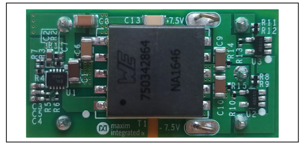
This reference design is derived from the MAX17681AEVKITE. The three main differences between MAXREFDES1169 and the MAX17681AEVKITE are as follows:
- The board size of the MAXREFDES1169 is 20mm × 40mm, which is approximately one-quarter the size of the MAX17681AEVKITE.
- The pin distances of the MAXREFDES1169 are consistent with Distributed-power Open Standards Alliance (DOSA) open standards for DC/DC brick power supplies.
- The reference design has two transformer options, one is from Würth Elektronik® and the other is from the transformer vendor HanRun Electronics®.
With the above three features, customers can reduce the whole solution size and cost. Customers can also mount this reference design on system boards.
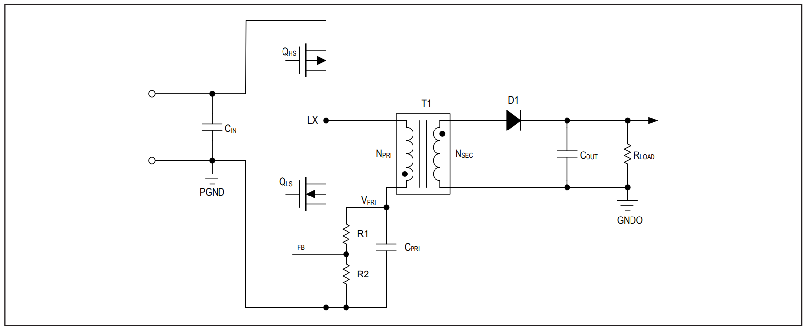
The iso-buck has a synchronous-buck-converter-based topology, useful for generating isolated outputs at low power levels without using an optocoupler. Figure 2 shows the basic circuit of an iso-buck converter, comprising a half-bridge transformer driver and secondary side filter.
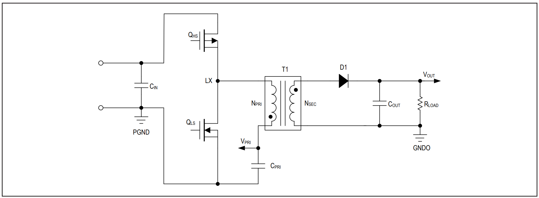
Figure 3 shows the equivalent circuit when the highside switch (QHS) is on. During this time, the primary current ramps up and stores energy in the transformer magnetizing inductance (LPRI) and the primary capacitor (CPRI) The secondary side diode is reverse-biased, and the load current is supplied by the secondary-side filter capacitor (COUT).
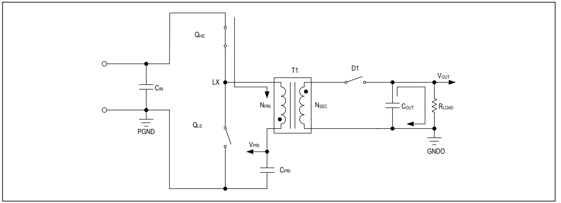
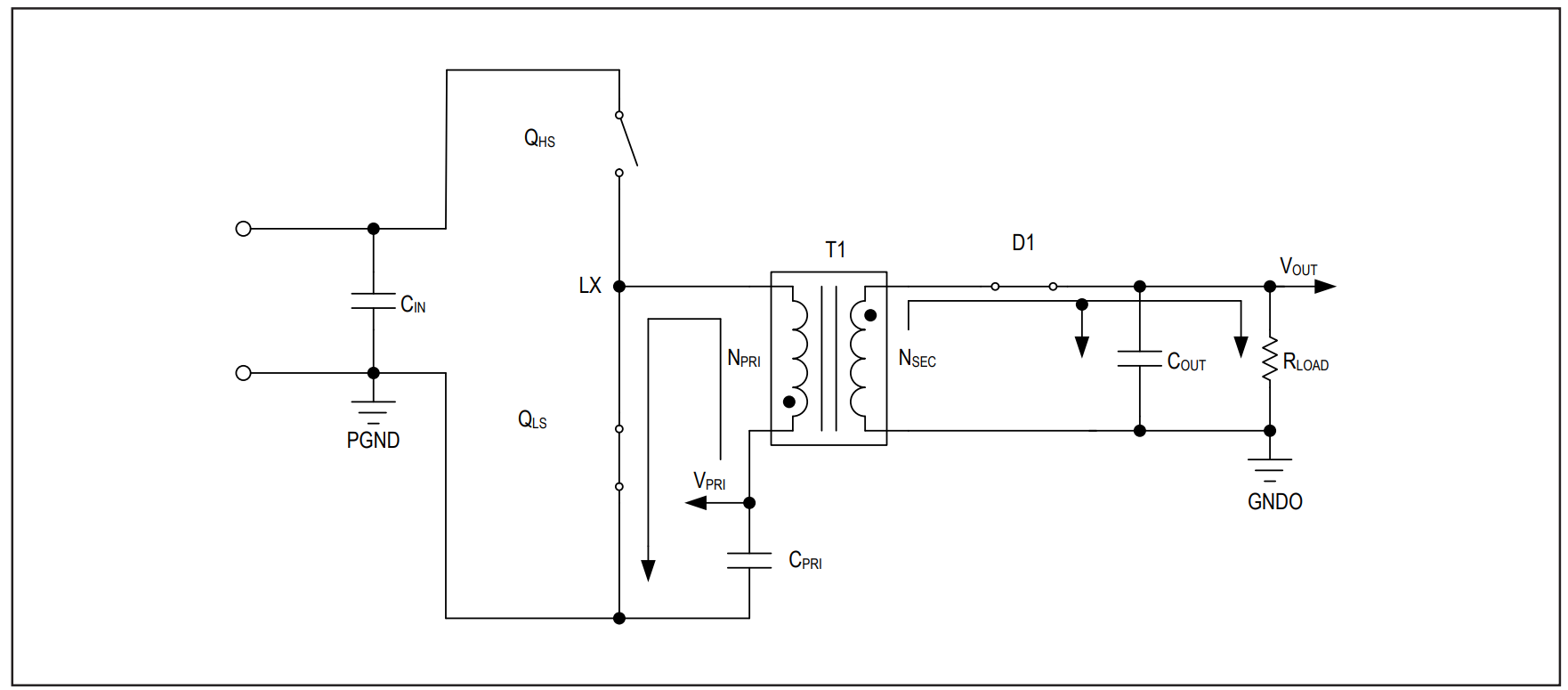
Figure 4 shows the equivalent circuit when the low-side switch (QLS) is on. During this time, the secondary diode gets forward-biased. The primary current ramps down and releases stored energy in the transformer magnetizing inductance and the primary capacitor to the load.
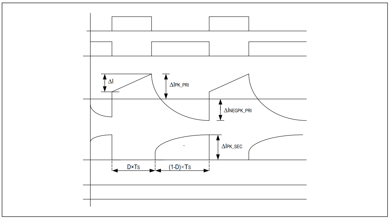
Operating waveforms of the converter are shown in Figure 5. Neglecting diode drop VD, transformer resistances, and leakage inductance, the output voltage VOUT is proportional to the primary output voltage CPRI and is regulated by the MAX17681/MAX17681A control loop.
Design Procedure for the Iso-Buck Converter
Now that the principle of operation of the iso-buck is understood, a practical design example can be illustrated. The converter design process can be divided into different stages, such as power stage design and setup of the MAX17681 iso-buck peak current mode controller. This document is primarily concerned with the power stage design, and the other circuit is intended to complement the information contained in the MAX17681 data sheet for details on how to set up the protection functions of the controller.
The following design parameters are used throughout:
| SYMBOL | FUNCTION |
| VIN | Input voltage |
| VINU | Input Under-Voltage Lockout Level |
| tSS | Soft Start Time |
| VO | Output Voltage |
| ∆I | Primary Ripple Current |
| IO | Output Current |
| fSW | Switching Frequency |
| DMAX | Maximum Duty Cycle |
| K | Secondary to Primary Turns Ratio |
| VPRI | Primary Voltage |
| IPK_PRI | Primary Peak Current |
| IPRI_RMS | Primary RMS Current |
| IPK_SEC | Secondary Peak Current |
| IPRI_RMS | Secondary RMS Current |
The above symbols are sometimes followed by parentheses to indicate whether minimum or maximum values of the parameters are intended, for example: minimum input voltage is intended by the symbol VIN(MIN). Otherwise typical values are intended. In addition, through the design procedure reference is made to the schematic in another document.
Step 1: Primary Output Voltage Selection
Primary output voltage is regulated by the MAX17681/ MAX17681A control loop. The primary output voltage can be calculated by using the following equation:
VPRI = DMAX x VIN(MIN)
where DMAX is the maximum duty cycle of the converter and VIN(MIN) is the minimum input voltage. Maximum duty cycle should be in the range of 0.4 to 0.6 for ideal iso-buck operation. In this design we use 0.5 as the maximum duty cycle, so
VPRI = 0.5 x 17 = 8.5V
Step 2: Adjusting the Primary Output Voltage
The primary output voltage is set with a resistor-divider from the primary output to FB to GND (see Figure 6). Choose R2 in the range of 10k to 49.9k and calculate R1 using the equation:

Choose R2 = 11k, so:

Choose R1 = 86.6k, so VPRI = 7.99V
Step 3: Transformer Turns Ratio Selection
Neglecting the diode drop VD, transformer resistances, and leakage inductance, the iso-buck output voltage VOUT is proportional to the primary output voltage VPRI. The turns ratio (K) is given by the following equation:

The turns ratio can be adjusted to match the readily available off-the-shelf transformer turns ratio by adjusting the primary output voltage.
There are four output voltages in this design, so four secondary coils are needed. We use K1 as the turns ratio of the +15V output voltage and the primary output voltage, K2 as the turns ratio of the -15V output voltage and the primary output voltage, K3 as the turns ratio of the +7.5V output voltage and the primary output voltage, and K4 as the turns ratio of the -7.5V output voltage and the primary output voltage, so

Choose K1 = 2, K2 = 2, K3 = 1, and K4 = 1.
Step 4: Primary Inductance Selection
The primary inductance value determines the ripple current in the transformer. The required primary inductance is given by the equation:
LPRI = 7 x VPRI = 7 x 7.99 = 55.93µH
where LPRI is the primary inductance in μH and VPRI is the primary output voltage. Choose LPRI = 50µH. The primary ripple current can be calculated using the following equation:

where LPRI is the primary inductance in H, fSW is the switching frequency in Hz, VPRI is the primary output voltage, VIN is the input voltage.
Step 5: Winding Peak and RMS Currents Calculation
The winding peak and RMS current ratings should be specified for selecting the iso-buck transformer. Primary and secondary winding peak currents are given by the following equations:

Where n is the total number of isolated outputs, i is the individual isolated output, IO is the secondary load current, K is the secondary turns ratio, D is the duty cycle, and ΔI is the primary ripple current. Primary RMS current is the sum of the high-side and low-side switch RMS currents.
The high-side switch RMS current is given by the following equation:

The low-side switch RMS current is given by the following equation:

The primary winding RMS current is given by the following equation:

The secondary winding RMS current is given by the following equation:

Step 6: Leakage Inductance
Transformer leakage inductance (LLEAK) plays a key role in determining the output voltage regulation. For better output voltage regulation, leakage inductance should be reduced to less than 1% of the primary inductance value. Higher leakage inductance also limits the amount of power delivered to the output.
Step 7: Primary Output Capacitor Selection
X7R ceramic output capacitors are preferred, due to their stability over temperature in industrial applications. The minimum required output capacitance is given by the following equation:

Step 8: Secondary Output Capacitor Selection
A secondary side capacitor supplies load current when the high-side switch is on. The required output capacitance to support 1% steady state ripple is given by the following equation:

Dielectric materials used in ceramic capacitors exhibit capacitance loss due to DC bias levels and should be appropriately derated to ensure the required output capacitance is obtained in the application.
Step 9: Input Capacitor Selection
Ceramic input capacitors are recommended for the IC. The input capacitor reduces peak current drawn from the power source and reduces noise and voltage ripple on the input caused by the switching circuitry. In applications where the source is located distant from the device input, an electrolytic capacitor should be added in parallel to the input ceramic capacitor to provide necessary damping for potential oscillations caused by the longer input power path and input ceramic capacitor. The required input capacitance can be calculated using the following equation:

∆VIN is the input voltage ripple, normally 2% of the minimum input voltage, DMAX is the maximum duty cycle, and fSW is the switching frequency of operation.
Step 10: Secondary Diode Selection
A secondary rectifier diode should be rated to carry peak secondary current and to withstand reverse voltage when the high-side switch is on. A Schottky diode with less forward-voltage drop should be selected for better output voltage regulation. The peak current rating of the diode is given by the following equation:

The peak reverse voltage rating of the diode is given by the following equations:

Step 11: Soft-Start Capacitor Selection
The MAX17681/MAX17681A implements an adjustable soft-start operation to reduce inrush current. A capacitor connected from the SS pin to GND programs the soft-start period. The soft-start time (tSS) is related to the capacitor connected at SS (CSS) by the following equation:
CSS = 5.55 × tSS
where tSS is in milliseconds and CSS is in nanofarads.
Step 12: Input Under-Voltage Lockout Level Setting
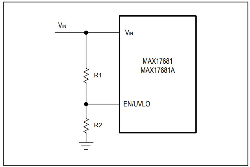
The device offers an adjustable input under-voltage-lockout level. Set the voltage at which the device turns on with a resistive voltage-divider connected from VIN to GND (see Figure 7). Connect the center node of the divider to EN/UVLO. Choose R1 to be 3.3MΩ max and then calculate R2 as follows:

where VINU is the voltage at which the device is required to turn on. Choose R1 = 3.01MΩ, VINU = 14V, so R2 = 261kΩ.
文件和资源
-
MAXREFDES1169 Design Files2019/7/9ZIP2 M
支持与培训
搜索我们的知识库,获取技术问题答案。我们专门的应用工程师团队也会随时为您解答技术问题。