


概览
设计资源
描述
The MAX17596 is a peak-current-mode controller for designing wide input-voltage flyback regulators. The device offers input thresholds suitable for low-voltage DC-DC applications (4.5V to 36V) and contains a built-in gate driver for an external n-channel MOSFET. The MAX17596 houses an internal error amplifier with 1% accurate reference, eliminating the need for an external reference. The switching frequency is programmable from 100kHz to 1MHz with an accuracy of 8%, allowing optimization of magnetic and filter components, resulting in compact and cost-effective power conversion. For EMI-sensitive applications, the MAX17596 incorporates a programmable frequency dithering scheme, enabling low-EMI spread-spectrum operation. Users can start the power supply precisely at the desired input voltage, implement input overvoltage protection, and program soft-start time. A programmable slope compensation scheme is provided to ensure stability of the peak current-mode control scheme. Hiccup-mode overcurrent protection and thermal shutdown are provided to minimize dissipation in overcurrent and overtemperature fault conditions.
优势和特点
- Programmable Switching Frequency Allows Optimization of the Magnetic and Filter Components, Resulting in Compact, Cost-Effective, Efficient Isolated/Nonisolated Power Supplies
- 100kHz to 1MHz Programmable Switching Frequency with Optional Synchronization
- Peak Current Mode Control Provides Excellent Transient Response
- Programmable Frequency Dithering Enables Low EMI Spread-Spectrum Operation
- Integrated Protection Features Enhance System Reliability
- Adjustable Current Limit with External Current-Sense Resistor
- Fast Cycle-By-Cycle Peak Current Limiting
- Overtemperature Protection
- Programmable Soft-Start and Slope Compensation
- Input Overvoltage Protection
所用产品
详情
The MAX17596 is a peak-current-mode controller for designing wide input-voltage flyback regulators. The device offers input thresholds suitable for low-voltage DC-DC applications (4.5V to 36V) and contains a built-in gate driver for an external n-channel MOSFET. The MAX17596 houses an internal error amplifier with 1% accurate reference, eliminating the need for an external reference. The switching frequency is programmable from 100kHz to 1MHz with an accuracy of 8%, allowing optimization of magnetic and filter components, resulting in compact and cost-effective power conversion. For EMI-sensitive applications, the MAX17596 incorporates a programmable frequency dithering scheme, enabling low-EMI spread-spectrum operation. Users can start the power supply precisely at the desired input voltage, implement input overvoltage protection, and program soft-start time. A programmable slope compensation scheme is provided to ensure stability of the peak current-mode control scheme. Hiccup-mode overcurrent protection and thermal shutdown are provided to minimize dissipation in overcurrent and overtemperature fault conditions.
- Programmable Switching Frequency Allows Optimization of the Magnetic and Filter Components, Resulting in Compact, Cost-Effective, Efficient Isolated/Nonisolated Power Supplies
- 100kHz to 1MHz Programmable Switching Frequency with Optional Synchronization
- Peak Current Mode Control Provides Excellent Transient Response
- Programmable Frequency Dithering Enables Low EMI Spread-Spectrum Operation
- Integrated Protection Features Enhance System Reliability
- Adjustable Current Limit with External Current-Sense Resistor
- Fast Cycle-By-Cycle Peak Current Limiting Hiccup-Mode Short-Circuit Protection
- Overtemperature Protection
- Programmable Soft-Start and Slope Compensation
- Input Overvoltage Protection
A DC input DCM flyback converter using the MAX17596 is demonstrated for a 24V DC output application. The power supply delivers up to 100mA at 24V. Table 1 shows an overview of the design specification.
| Parameter | Symbol | Min | Max |
| Input Voltage | VIN | 19V | 29V |
| Frequency | fSW | 29V | |
| Maximum Efficiency | η | 87.8% | |
| Output Voltage | VOUT | 24V | |
| Output Voltage Ripple | ∆VOUT | 1% of VOUT (max) | |
| Output Current | IOUT | 0 | 100mA |
| Output Power | POUT | 2.4W | |
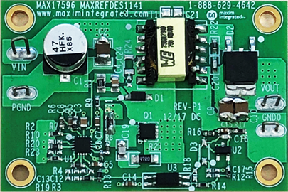
This document describes the hardware shown in Figure 1. It provides a detailed systematic technical guide to designing a DC-DC discontinuous conduction mode (DCM) flyback using Analog Devices MAX17596 current-mode controller. The power supply has been built and tested, details of which follow later in this document.
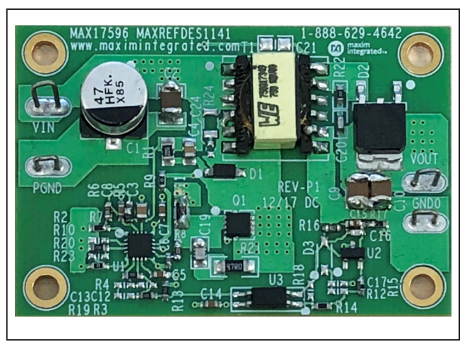
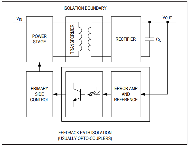
Figure 2 shows a generic isolated power-supply block diagram. It consists of a power stage, an isolation transformer, rectifier, secondary-side error amplifier, and opto-coupler to provide a feedback for the primary side control. Different isolated power supplies are different depending upon how the transformer is being used in them.
A transformer in a flyback configuration acts differently than its usual operation of transformation of energy from primary to secondary. During a transformer’s usual operation, both primary and secondary windings conduct together at the same time to make the transfer of energy possible from primary to secondary. In a flyback configuration the primary and secondary windings do not conduct at the same time and the transformer acts more like a coupled inductor. Note that in this document we have used the following notations for the transformer turns ratio:
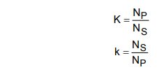
This means capital K for primary turns/secondary turns and small k for secondary turns/primary turns.
Figure 3 shows a simple flyback topology that consists of a transformer whose primary winding is connected to the drain of a switching MOSFET. The source of the MOSFET is connected to ground. The secondary winding is connected to the output capacitor through a rectifier diode. In this flyback configuration the current flows into the primary winding during the on time of the switching period and flows into the secondary winding during the off time of the switching period.
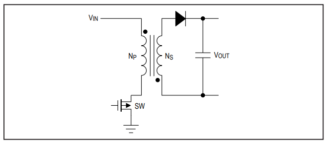
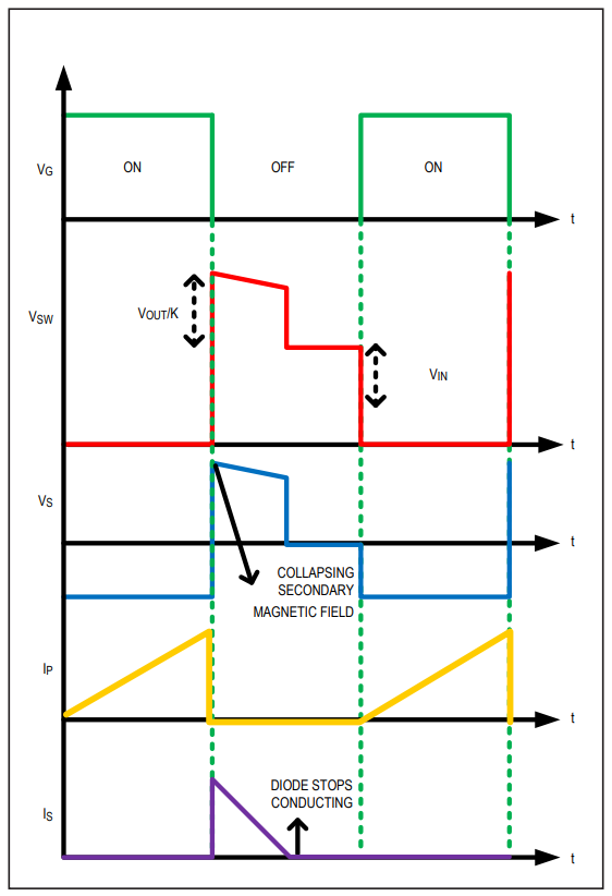
During the on-time when the primary switch is closed, a current, IP, flows through the primary winding as shown in Figure 4. IP can be written as follows:

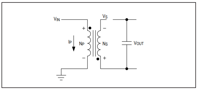
The peak magnitude of the primary current can be written as follows:

In the secondary winding, a negative voltage is induced due to the current flowing in to the primary. The rectifier diode is reverse-biased and no current is flowing in the secondary winding. The induced voltage in the primary can be written as:

During the off-time when the primary switch opens as shown in Figure 5, the magnetic field in the primary winding collapses and the voltage at the winding reverses, while current keeps flowing in the same direction until the field fades away.
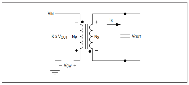
The secondary current IS flows and the secondary and rectifier diode is forward-biased. Output voltage VOUT is now available across the secondary coil if we ignore the forward voltage drop of the rectifier diode. The secondary winding voltage is now flown away to primary side as K x VOUT. This voltage is present across the switch until the current in the secondary winding decays to zero. Total voltage available across the switch during the off-time can be written as:

This voltage also causes the breakdown of the magnetic flux in the primary winding (no current is flowing in the primary winding after this reset). Here we can see that unlike a usual transformer action where current flows in both the winding at the same time, in a flyback transformer the current flows into the primary winding during the on-time and into the secondary winding during the off-time. This is why we use the term “coupled storage inductor” for transformers used in flyback operation. It should be noted though that mechanically these transformers are like any transformer. Use in flyback operations makes transformers act differently as coupled inductors. The required duty cycle for a given input voltage and output voltage can be calculated from:
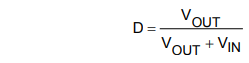
where:

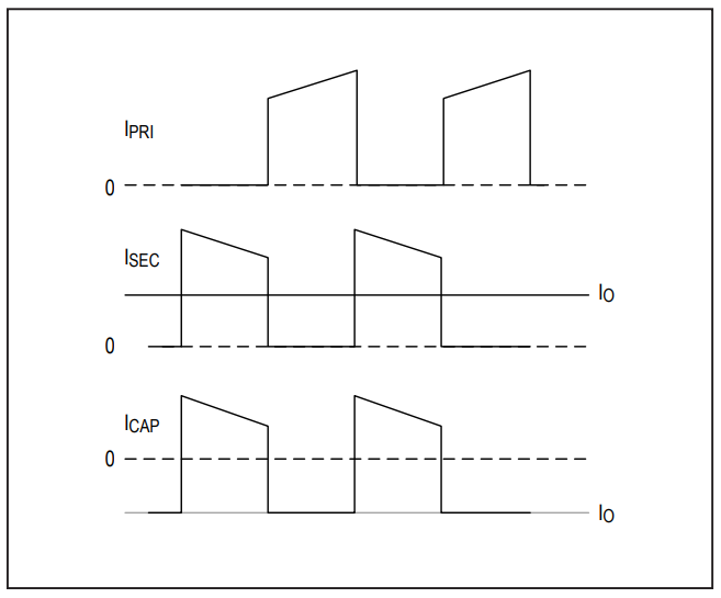
Figure 6 shows a typical CCM mode flyback primary and secondary winding current, and Figure 7 shows a typical DCM mode flyback waveform.
Design Procedure for DC-DC Flyback Using MAX17596
Now that the basic principle of the DCM flyback is understood, a practical design can be illustrated. The design parameters are obtained by using expressions given in Analog Devices Application Note 5504. This document is primarily concerned with the power stage and the feedback loop design, and is intended to complement the information contained in the MAX17596 data sheet.
Flyback converters can be operated in discontinuous conduction mode (DCM) or continuous conduction mode (CCM). The component choices, stress level in power devices, and controller design vary depending on the operating mode of the converter. The design discussed in this document is a DCM design and expressions for calculating component values and ratings are presented to achieve the design goals.
Step 1: Switching Frequency
For this design we selected a 150kHz switching frequency. The MAX17596 switching frequency is programmable between 100kHz and 1000kHz with a resistor RRT connected between RT and SGND. RRT is calculated as follows:
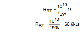
A standard 66.5kΩ resistor is selected for RRT.
Step 2: Transformer Magnetizing Inductance and Turns Ratio
In a DCM flyback converter, the energy stored in the primary inductance of the flyback transformer is delivered entirely to the output. The maximum primary-inductance value for which the converter remains in DCM at all operating conditions can be calculated as:
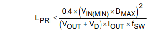
where:
DMAX = 0.43V
VD = 0.76V which is the forward voltage drop of the selected rectifier diode.
In this application, the DC input voltage varies from 19V DC to 29V DC. Substitute the values in the expression of LPRI as follows:

For our design LPRI is chosen as 70µH, LPRI = 70µH.
The leakage inductance of the transformer should be targeted as low as possible. For this design, we achieved a 1.5% leakage inductance of 1.05µH, LLKG = 1.05µH. A customized transformer 750317349 from Würth Elektronik® is used in this design. This transformer also fulfills the specification of turns ratio and primary/secondary currents requirement of the design that is calculated step by step in this document. The transformer has dielectric isolation specification of 1500V AC.
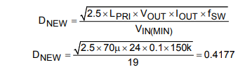
Step 3: Maximum Duty-Cycle Calculation with Selected LPRI
Use the following expressions to calculate the maximum duty cycle of the converter for the selected frequency and magnetizing inductance:
Calculate the required transformer turns ratio (k) using the expressions as follows:
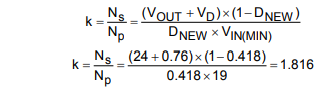
For the present design, k is chosen as 1:1.816.
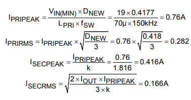
Step 4: Calculation of Peak/RMS Current
Primary and secondary RMS and primary peak currents calculations are needed to design the transformer in switched-mode power supplies. Also, primary peak current is used in setting the current limit. Use the following expressions to calculate the primary and secondary peak and RMS currents:
Step 5: Current-Limit Resistor Calculation
For the current-limit setting, the peak current can be calculated as follows:

The device includes a robust overcurrent protection scheme that protects the device under overload and short-circuit conditions. A current-sense resistor, connected between the source of the MOSFET and PGND, sets the peak current limit. The current-limit comparator has a voltage trip level (VCS-PEAK) of 300mV. Use the following equation to calculate the value of RCS:

where IMOSFET is the peak current flowing through the MOSFET. A typical 300mΩ current-sense resistor is selected, RCS = 300mΩ.
Step 6: MOSFET Selection
MOSFET selection criteria includes maximum drain voltage, peak/RMS current in the primary, and the maximum allowable power dissipation of the package without exceeding the junction temperature limits. The voltage seen by the MOSFET drain is the sum of the input voltage, the reflected secondary voltage on the transformer primary, and the leakage inductance spike. The MOSFET’s absolute maximum VDS rating must be higher than the worst-case drain voltage as follows:
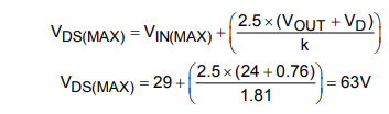
For this application we chose the Vishay® SQSA80ENWT1-GE3 80V, 18A n-channel MOSFET as the primary MOSFET.
Step 7: Snubber Selection
An RCD snubber reduces the maximum voltage stress on the MOSFET by clamping the voltage level. However, it also dissipates power and reduces efficiency. RCD snubbers may not always be required, however, it is always a good idea to leave place holders in the board for RCD and RC snubbers. Ideally, the external MOSFET experiences a drain-source voltage stress equal to the sum of the input voltage and reflected voltage across the primary winding during the off period of the MOSFET. In practice, parasitic inductors and capacitors in the circuit, such as leakage inductance of the flyback transformer, cause voltage overshoot and ringing in addition to the ideally expected voltage stress. Snubber circuits are used to limit the voltage overshoots to safe levels within the voltage rating of the external MOSFET. The snubber capacitor can be calculated using the following expression:
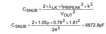
We selected a 6800pF capacitor, CSNUB = 6800pF.
The power that must be dissipated in the snubber resistor is calculated using the following expressions:

The snubber resistor is calculated based on the below expression:

A standard 15kΩ, 0.33W resistor is selected, RSNUB = 15kΩ.
The voltage rating of the snubber diode is:
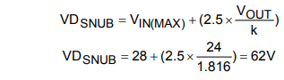
We selected the Micro Commercial Components® SMD110PL 100V, 1A diode as the snubber diode.
Step 8: Secondary Diode Selection
The maximum operating reverse voltage rating of the secondary rectifier diode must be higher than the sum of the output voltage and the reflected input voltage. We use the following expression to calculate the secondary diode voltage rating:

We selected STMicroelectronics® STTH4R02B 200V, 4A diode as the secondary side rectifier diode using MAX17606.
Step 9: Feedback Resistor (RU, RB) Selection
A standard 10kΩ resistor is selected, RB = 10kΩ.
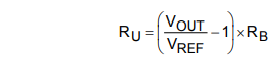
where VREF is the reference set by the secondary-side controller (VREF = 2.5V for TL431AQDBZRQ1 is used in this design).

A standard 86.6kΩ resistor is selected, RU = 86.6kΩ.
Step 10: Soft-Start Capacitor
The soft-start period for the devices can be programmed by selecting the value of the capacitor CSS connected from the SS pin to SGND. Capacitor CSS can be calculated as:

where tSS is expressed in ms and the resultant value of CSS is in nF.

A standard 100nF is selected as the soft-start capacitor, CSS = 100nF.
Step 11: Input Capacitor Selection
For DC-DC applications, X7R ceramic capacitors are recommended due to their stability over the operating temperature range. The effective series resistance (ESR) and effective series inductance (ESL) of a ceramic capacitor are relatively low, so the ripple voltage is dominated by the capacitive component. For the flyback converter, the input capacitor supplies the current when the main switch is on. We used the following equation to calculate the input capacitor for a specified peak-to-peak input switching ripple:
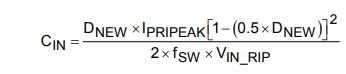
Step 12: Output Capacitor Selection
X7R ceramic output capacitors are preferred in industrial applications due to their stability over temperature. The output capacitor is usually sized to support a step load of a certain percentage of the rated output current so that the output voltage deviation is contained to 3% of the rated output voltage. The output capacitance can be calculated by using the below expressions:

where ISTEP is the load step, tRESPONSE is the response time of the controller, ∆VOUT is the allowable output voltage deviation, and fC is the target closed-loop crossover frequency. In our application, we selected fC = 5kHz.
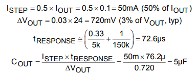
Due to the DC-bias characteristics, 2 x 4.7µF 50V MLCC capacitors are selected for this design.
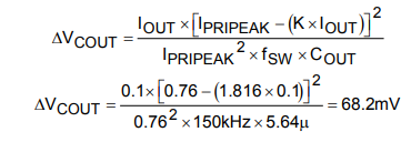
Capacitor values change with temperature and applied voltage. Refer to the capacitor data sheets to select capacitors that guarantee the required output capacitance across the operating range. For design calculations, use the worst-case derated value of capacitance, based on temperature range and applied voltage. In our case the worst-case derated value of capacitors is 5.64µF.
For the flyback converter, the output capacitor supplies the load current when the main switch is on, and therefore the output voltage ripple is a function of load current and duty cycle. Use the following expression to estimate the output capacitor ripple:
Step 13: Loop Compensation
Optocoupler feedback is used in isolated flyback converter designs for precise control of isolated output voltage. Figure 8 shows the overall scheme of the optocoupler feedback.
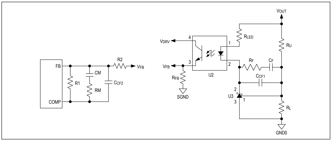
Use RFB = 470Ω (typ), for an optocoupler transistor current of 1mA. Select R1 = 49.9kΩ and R2 = 22kΩ (typical values) to use the full range of available COMP voltage. U3 is a low-voltage adjustable shunt regulator with a 2.5V reference voltage. In this design we selected a Texas Instruments® TL431AQDBZRQ1 2.5V shunt regulator.
Calculate RLED using the below expression:

A standard 8.66kΩ resistor is selected, RLED = 8.66kΩ.
The bandwidth of typical optocouplers limits the achievable closed-loop bandwidth of opto-isolated converters. Considering this limitation, the closed-loop crossover frequency can be chosen at the nominal input voltage by selecting fC = 5kHz. Closed-loop compensation values are designed based on the open-loop gain at the desired crossover frequency, fC. The open-loop at fC is calculated using the following expressions.
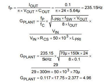
Three controller configurations are suggested in Application Note 5504 based on open-loop gain and the RLED value. For typical designs, the current transfer ratio (CTR) of the optocoupler designs can be assumed to be unity. It is known that the comparator and gate-driver delays associated with the input voltage variations affect the optocoupler CTR. Depending on the optocoupler selected, variations in CTR causes wide variations in bandwidth of the closed-loop system across the input-voltage operating range. It is recommended to select an optocoupler with less CTR variations across the operating range. Checking the condition as stated in Application Note 5504:
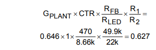
As stated in Application Note 5504, as 0.627 < 0.8, configuration 1 is selected. Figure 9 shows a typical schematic of configuration 1. The RF value can be calculated from the expression below:

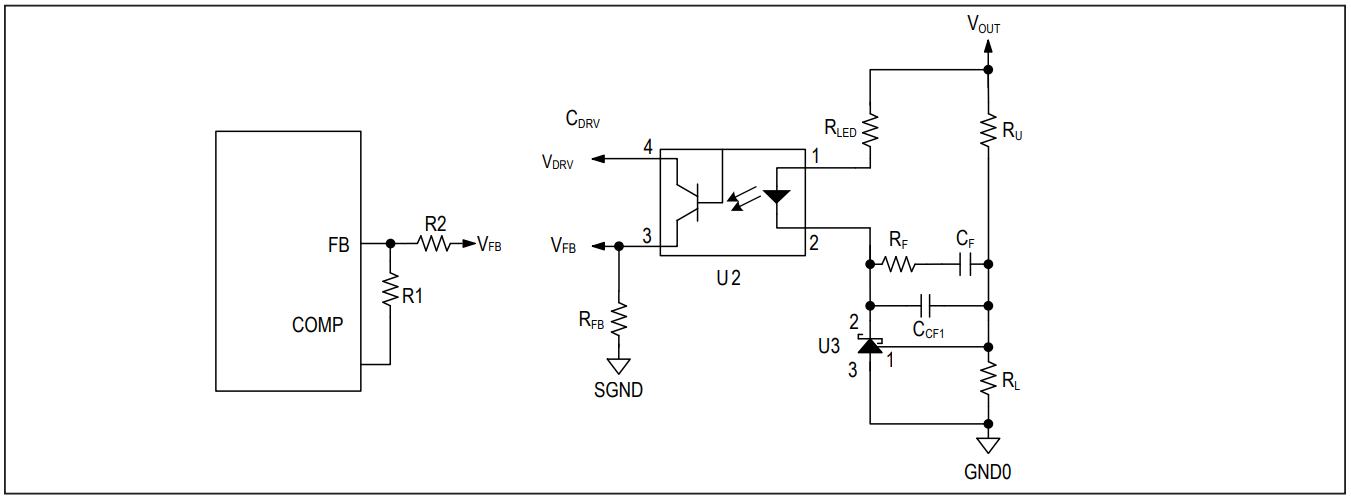
A typical 56k value is selected as RF, RF = 56kΩ.
The CF value can be calculated as follows:
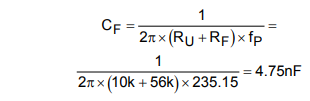
A standard 4.7nF capacitor is selected, CF = 4.7nF.
The CCF1 value can be calculated as follows:
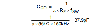
A standard 39pF capacitor is selected, CCF1 = 39pF.
Step 14: EN/UVLO and OVI Setting
The device’s EN/UVLO pin serves as an enable/disable input, as well as an accurate programmable input UVLO pin. The device does not commence startup operation unless the EN/UVLO pin voltage exceeds 1.21V. The device turns off if the EN/UVLO pin voltage falls below 1.15V. A resistor-divider from the input DC bus to ground can be used to divide down and apply a fraction of the input DC voltage (VDC) to the EN/UVLO pin. The values of the resistor-divider can be selected so the EN/UVLO pin voltage exceeds the 1.23V turn-on threshold at the desired input DC bus voltage. The same resistor-divider can be modified with an additional resistor (ROVI) to implement input overvoltage protection in addition to the EN/UVLO functionality as shown in Figure 10.
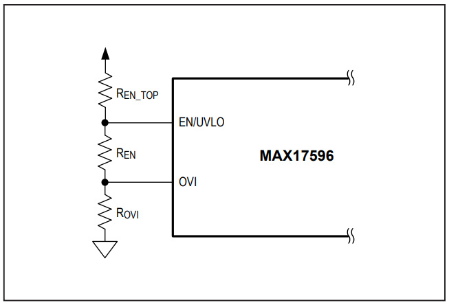
When voltage at the OVI pin exceeds 1.21V, the device stops switching and resumes switching operations only if voltage at the OVI pin falls below 1.15V. For given values of startup DC input voltage (VSTART) and input overvoltage-protection voltage (VOVI), the resistor values for the divider can be calculated as follows:
Select ROVI = 10kΩ.
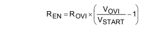
where VOVI = maximum allowed overvoltage = 33V.

A standard 7.5kΩ resistor is selected, REN = 7.5kΩ.
The same resistor-divider can be modified to implement input overvoltage protection. When the voltage at the OVI pin exceeds 1.215V (typ), the device stops switching. The device resumes switching operations only if the voltage at the OVI pin falls below 1.1V (typ).
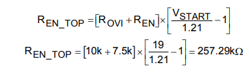
A standard 261kΩ resistor is selected for REN_TOP.
文件和资源
-
MAXREFDES1141 Design Files2019/7/9ZIP2 M
-
MAXREFDES1141: 2.4W DC-DC Flyback Converter Using the MAX175962019/7/9PDF530K
支持与培训
搜索我们的知识库,获取技术问题答案。我们专门的应用工程师团队也会随时为您解答技术问题。