
MAXREFDES1090
Miniature, 12V/250mA, No-Opto Flyback DC-DC Converter with 91.3% Efficiency Using the MAX17690


概览
设计资源
描述
Due to its simplicity and low cost, the flyback converter is the preferred choice for low-to-medium isolated DC-DC power-conversion applications. However, the use of an optocoupler or an auxiliary winding on the flyback transformer for voltage feedback across the isolation barrier increases the number of components and design complexity. The MAX17690 eliminates the need for an optocoupler or auxiliary transformer winding and achieves ±5% output voltage regulation over line, load, and temperature variations.
The MAX17690 implements an innovative algorithm to accurately determine the output voltage by sensing the reflected voltage across the primary winding during the flyback time interval. By sampling and regulating this reflected voltage when the secondary current is close to zero, the effects of secondary-side DC losses in the transformer winding, the PCB tracks, and the rectifying diode on output voltage regulation can be minimized.
The MAX17690 also compensates for the negative temperature coefficient of the rectifying diode.
优势和特点
- 4.5V to 60V Input Voltage Range
- Programmable Switching Frequency from 50kHz to 250kHz
- Programmable Input Enable/UVLO Feature
- Programmable Input Overvoltage Protection
- Adjustable Soft-Start
- 2A/4A Peak Source/Sink Gate Drive Capability
- Hiccup Mode Short-Circuit Protection
- Fast Cycle-by-Cycle Peak Current Limit
- Thermal Shutdown Protection
- Space-Saving, 16-Pin, 3mm x 3mm TQFN Package
- -40°C to +125°C Operating Temperature Range
所用产品
详情
Due to its simplicity and low cost, the flyback converter is the preferred choice for low-to-medium isolated DC-DC power-conversion applications. However, the use of an optocoupler or an auxiliary winding on the flyback transformer for voltage feedback across the isolation barrier increases the number of components and design complexity. The MAX17690 eliminates the need for an optocoupler or auxiliary transformer winding and achieves ±5% output voltage regulation over line, load, and temperature variations.
The MAX17690 implements an innovative algorithm to accurately determine the output voltage by sensing the reflected voltage across the primary winding during the flyback time interval. By sampling and regulating this reflected voltage when the secondary current is close to zero, the effects of secondary-side DC losses in the transformer winding, the PCB tracks, and the rectifying diode on output voltage regulation can be minimized.
The MAX17690 also compensates for the negative temperature coefficient of the rectifying diode.
Other features include the following:
- 4.5V to 60V Input Voltage Range
- Programmable Switching Frequency from 50kHz to 250kHz
- Programmable Input Enable/UVLO Feature
- Programmable Input Overvoltage Protection
- Adjustable Soft-Start
- 2A/4A Peak Source/Sink Gate Drive Capability
- Hiccup Mode Short-Circuit Protection
- Fast Cycle-by-Cycle Peak Current Limit
- Thermal Shutdown Protection
- Space-Saving, 16-Pin, 3mm x 3mm TQFN Package
- -40°C to +125°C Operating Temperature Range
An isolated no-opto flyback DC-DC converter using the MAX17690 is demonstrated for a 12V DC output application. The power supply delivers up to 250mA at 12V. Table 1 shows an overview of the design specification.
| Parameter | Symbol | Min | Max |
| Input Voltage | VIN | 8V | 28V |
| Frequency | fSW | 143.5kHz | |
| Peak Efficiency at Full Load | ηMAX | 91.3% | |
| Efficiency at Minimum Load | ηMIN | 60% | |
| Output Voltage | VOUT | 12V | |
| Output Voltage Ripple | ∆VO | 120mV | |
| Maximum Output Current | IOUT | 250mA | |
| Maximum Output Power | POUT | 3W | |
This document describes the hardware shown in Figure 1. It provides a detailed systematic technical guide to designing an isolated no-opto flyback DC-DC converter using Analog Devices MAX17690 controller. The power supply has been built and tested.
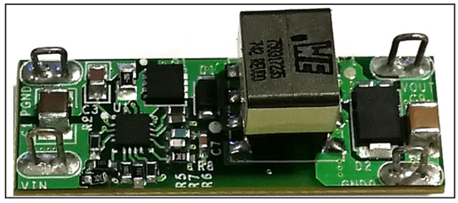
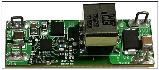
One of the drawbacks encountered in most isolated DC-DC converter topologies is that information relating to the output voltage on the isolated secondary side of the transformer must be communicated back to the primary side to maintain output voltage regulation. In a regular isolated flyback converter, this is normally achieved using an optocoupler feedback circuit or an additional auxiliary winding on the flyback transformer. Optocoupler feedback circuits reduce overall power-supply efficiency, and the extra components increase the cost and physical size of the power supply. In addition, optocoupler feedback circuits are difficult to design reliably due to their limited bandwidth, nonlinearity, high CTR variation, and aging effects. Feedback circuits employing auxiliary transformer windings also exhibit deficiencies. Using an extra winding adds to the flyback transformer’s complexity, physical size, and cost, while load regulation and dynamic response are often poor.
The MAX17690 is a peak current-mode controller designed specifically to eliminate the need for optocoupler or auxiliary transformer winding feedback in the traditional isolated flyback topology, therefore reducing size, cost, and design complexity. It derives information about the isolated output voltage by examining the voltage on the primary-side winding of the flyback transformer.
Other than this uniquely innovative method for regulating the output voltage, the no-opto isolated flyback converter using the MAX17690 follows the same general design process as a traditional flyback converter. To understand the operation and benefits of the no-opto flyback converter it is useful to review the schematic and typical waveforms of the traditional flyback converter (using the MAX17595), shown in Figure 2.
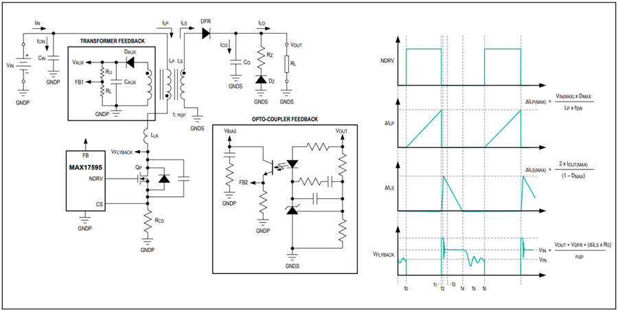
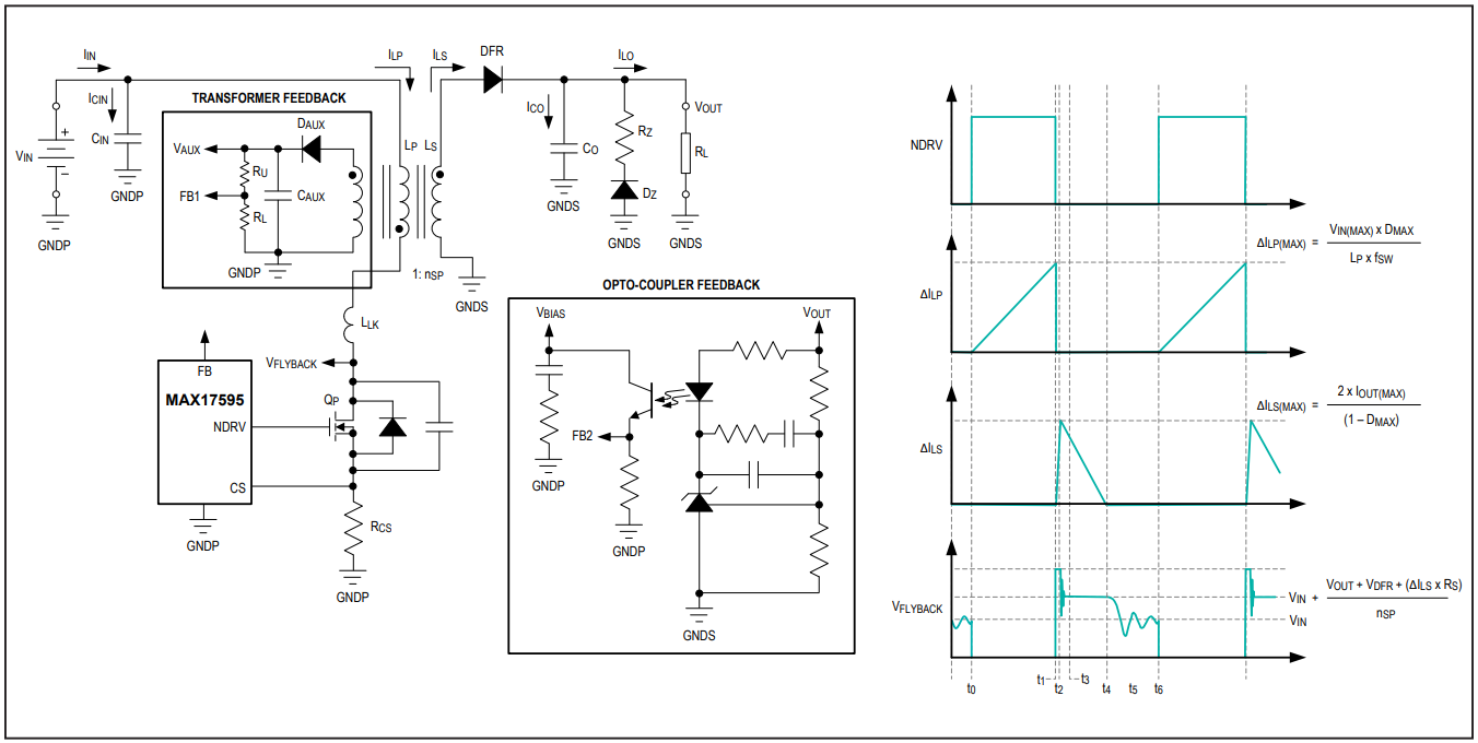
The simplified schematic in Figure 2 illustrates how information about the output voltage is obtained across the isolation barrier in traditional isolated flyback converters. The optocoupler feedback mechanism requires at least 10 components including an optocoupler and a shunt regulator, in addition to a primary-side bias voltage, VBIAS, to drive the photo-transistor. The error voltage FB2 connects to the FB pin of the flyback controller.
The transformer feedback method requires an additional winding on the primary side of the flyback transformer, a diode, a capacitor, and two resistors to generate a voltage proportional to the output voltage. This voltage is compared to an internal reference in a traditional flyback controller to generate the error voltage.
By including additional innovative features internally in the MAX17690 no-opto flyback controller, Analog Devices has enabled power-supply designers to eliminate the additional components, board area, complexity, and cost associated with both the optocoupler and transformer feedback methods. Figure 3 illustrates a simplified schematic and typical waveforms for an isolated no-opto flyback DC-DC converter using the MAX17690.
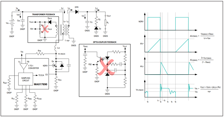
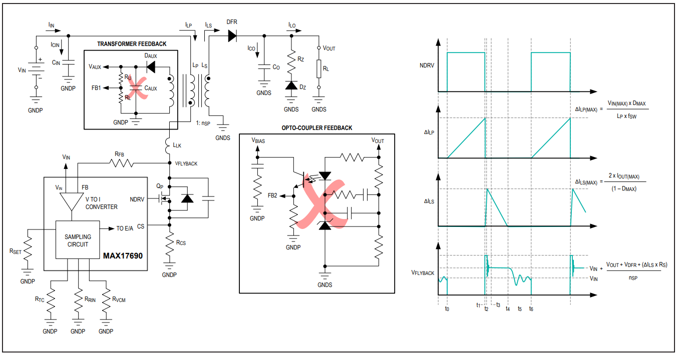
By comparing Figure 3 with Figure 2, it is evident that there is no difference in the voltage and current waveforms in the traditional and no-opto flyback topologies. The difference is in the control method used to maintain VOUT at its target value over the required load, line, and temperature range. The MAX17690 achieves this with minimum components by forcing the voltage VFLYBACK during the conduction period of DFR to be precisely the voltage required to maintain a constant VOUT. When QP turns off, DFR conducts and the drain voltage of QP, rises to a voltage VFLYBACK above VIN. After initial ringing due to transformer leakage inductance and the junction capacitance of DFR and output capacitance of QP, the voltage VFLYBACK is given by:

where:
VFLYBACK is the QP drain voltage relative to primary ground VDFR(T) is the forward voltage drop of DFR, which has a negative temperature coefficient
ILS(t) is the instantaneous secondary transformer current RS(T) is the total DC resistance of the secondary circuit, which has a positive temperature coefficient
nSP is the secondary to primary turns ratio of the flyback transformer
The voltage of interest is (VFLYBACK - VIN) since this is a measure of VOUT. An internal voltage to current amplifier generates a current proportional to (VFLYBACK - VIN). This current then flows through RSET to generate a ground referenced voltage, VSET, proportional to (VFLYBACK - VIN). This requires that:
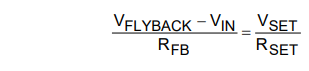
Combining this equation with the previous equation for VFLYBACK, we have:

We need to consider the effect of the temperature dependence of VDFR and the time dependence of ILS on the control system. If VFLYBACK is sampled at a time when ILS is very close to zero, then the term ILS(t) x RS(T) is negligible and can be assumed to be zero in the previous expression. This is the case when the flyback converter is operating in, or close to, discontinuous conduction mode. It is very important to sample the VFLYBACK voltage before the secondary current reaches zero since there is a very large oscillation on VFLYBACK due to the resonance between the primary magnetizing inductance of the flyback transformer and the output capacitance of QP as soon as the current reaches zero in the secondary, as shown in Figures 2 and 3. The time at which VFLYBACK is sampled is set by resistor RVCM.
The VDFR term has a significant negative temperature coefficient that must be compensated to ensure acceptable output voltage regulation over the required temperature range. This is achieved by internally connecting a positive temperature coefficient current source to the VSET pin. The current is set by resistor RTC connected to ground. The simplest way to understand the temperature compensation mechanism is to think about what needs to happen in the control system when temperature increases. In an uncompensated system, as the temperature increases, VDFR decreases due to its negative temperature coefficient. Since VDFR decreases, VOUT increases by the same amount, therefore VFLYBACK remains unchanged. Since VSET is proportional to VFLYBACK, VSET also remains unchanged. Since there is no change in VSET there is no change in duty cycle demand to bring VOUT back down to its target value. What needs to happen in the temperature compensated case is, when VOUT increases due to the negative temperature coefficient of VDFR, VSET needs to increase by an amount just sufficient to bring VOUT back to its target value. This is achieved by designing VSET with a positive temperature coefficient. Expressed mathematically as:
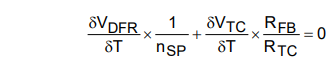
where:
δVDFR/δT is the diodes forward temperature coefficient
δVTC/δT = 1.85mV/°C
VTC = 0.55V is the voltage at the TC pin at +25°C
Rearranging the above expression gives:

The effect of adding the positive temperature coefficient current, TC, to the current in RFB is equivalent to adding a positive temperature coefficient voltage in series with VDFR on the secondary side of value:

Substituting from the previous expression, this becomes:
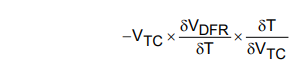
Now substituting this expression into the expression for VOUT gives:

and finally solving for RFB:

Values for RSET, VSET, and δVTC/δT can be obtained from the MAX17690 data sheet as follows:
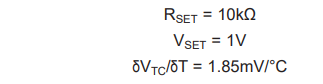
Values for VDFR and δVDFR/δT can be obtained from the output diode data sheet, and nSP is calculated when the flyback transformer is designed.
The value of RTC can then be calculated using the expression from earlier, restated below:

The calculated resistor values for RFB and RTC should always be verified experimentally and adjusted, if necessary, to achieve optimum performance over the required temperature range. Note that the reference design described in this document has only been verified at room temperature. Finally, the internal temperature compensation circuitry requires a current proportional to VIN. RRIN should be chosen as approximately:

Setting the VFLYBACK Sampling Instant
The MAX17690 generates an internal voltage proportional to the on-time volt-second product. This enables the device to determine the correct sampling instant for VFLYBACK during the QP off-time. The RVCM resistor is used to scale this internal voltage to an acceptable internal voltage limit in the device.
文件和资源
-
MAXREFDES1090 Design Files2021/2/15ZIP2M
支持与培训
搜索我们的知识库,获取技术问题答案。我们专门的应用工程师团队也会随时为您解答技术问题。