

概览
设计资源
描述
The MAX17690 is a peak current mode, fixed-frequency switching controller specifically designed for the isolated flyback topology operating in Discontinuous Conduction Mode (DCM). The device senses the isolated output voltage directly from the primary-side flyback waveform during the off-time of the primary switch. No auxiliary winding or optocoupler is required for output voltage regulation.
The MAX17690 is designed to operate over a wide supply range from 4.5V to 60V. The switching frequency is programmable from 50kHz to 250kHz. The MAX17690 provides an input overvoltage protection through the OVI pin. The 7V internal LDO output of the MAX17690 makes it suitable for switching both logic-level and standard MOSFETs used in flyback converters. With 2A/4A source/ sink currents, the MAX17690 is ideal for driving low RDS(ON) power MOSFETs with fast gate transition times. The MAX17690 provides an adjustable soft-start feature to limit the inrush current during startup.
The MAX17690 provides temperature compensation for the output diode forward-voltage drop. The MAX17690 has robust hiccup-protection and thermal protection schemes, and is available in a space-saving 3mm x 3mm 16-pin TQFN package with a temperature range from -40°C to +125°C.
优势和特点
- No Optocoupler or Third Winding Required
- 2A/4A Peak Source/Sink Gate Drive Currents
- 50kHz to 250kHz Programmable Switching Frequency
- Input EN/UVLO Feature
- Input Overvoltage Protection
- Programmable Soft-Start
- Hiccup-Mode Short-Circuit Protection
- Thermal Shutdown Protection
- -40°C to +125°C Operating Temperature Range
- Space-Saving, 3mm x 3mm, 16-Pin TQFN Package
所用产品
详情
The MAX17690 is a peak current mode, fixed-frequency switching controller specifically designed for the isolated flyback topology operating in Discontinuous Conduction Mode (DCM). The device senses the isolated output voltage directly from the primary-side flyback waveform during the off-time of the primary switch. No auxiliary winding or optocoupler is required for output voltage regulation.
The MAX17690 is designed to operate over a wide supply range from 4.5V to 60V. The switching frequency is programmable from 50kHz to 250kHz. The MAX17690 provides an input overvoltage protection through the OVI pin. The 7V internal LDO output of the MAX17690 makes it suitable for switching both logic-level and standard MOSFETs used in flyback converters. With 2A/4A source/ sink currents, the MAX17690 is ideal for driving low RDS(ON) power MOSFETs with fast gate transition times. The MAX17690 provides an adjustable soft-start feature to limit the inrush current during startup.
The MAX17690 provides temperature compensation for the output diode forward-voltage drop. The MAX17690 has robust hiccup-protection and thermal protection schemes, and is available in a space-saving 3mm x 3mm 16-pin TQFN package with a temperature range from -40°C to +125°C.
- No Optocoupler or Third Winding Required
- 2A/4A Peak Source/Sink Gate Drive Currents
- 50kHz to 250kHz Programmable Switching Frequency
- Input EN/UVLO Feature
- Input Overvoltage Protection
- Programmable Soft-Start
- Hiccup-Mode Short-Circuit Protection
- Thermal Shutdown Protection
- -40°C to +125°C Operating Temperature Range
- Space-Saving, 3mm x 3mm, 16-Pin TQFN Package
A no-opto flyback DC-DC converter using the MAX17690 is demonstrated for a 54V DC output application. The power supply delivers up to 1.1A at 54V. Table 1 shows an overview of the design specification.
| Parameter | Symbol | Min | Max |
| Input Voltage | VIN | 18V | 60V |
| Frequency | fSW | 125kHz | |
| Maximum Efficiency | η | 91% | |
| Output Voltage | VOUT | 54V | |
| Output Current | IOUT | 0A | 1.1A |
| Output Power | POUT | 59.4W | |
This document describes the hardware shown in Figure 1. It provides a detailed systematic technical guide to designing a no-opto flyback using Analog Devices MAX17690 current-mode controller. The power supply has been built and tested, details of which follow later in this document.


Figure 2 shows a generic isolated power-supply block diagram. It consists of a power stage, an isolation transformer, rectifier, secondary-side error amplifier, and opto-coupler to provide a feedback for the primary side control. Different isolated power supplies are different depending upon how the transformer is being used in them.


A transformer in a flyback configuration acts differently than its usual operation of transformation of energy from primary to secondary. During a transformer’s usual operation, both primary and secondary windings conduct together at the same time to make the transfer of energy possible from primary to secondary. In a flyback configuration the primary and secondary windings do not conduct at the same time and the transformer acts more like a coupled inductor. Note that in this document we have used the following notations for the transformer turns ratio:

This means capital K for primary turns/secondary turns and small k for secondary turns/primary turns.
Figure 3 shows a simple flyback topology that consists of a transformer whose primary winding is connected to the drain of a switching MOSFET. The source of the MOSFET is connected to ground. The secondary winding is connected to the output capacitor through a rectifier diode. In this flyback configuration the current flows into the primary winding during the on time of the switching period and flows into the secondary winding during the off time of the switching period.


During the on-time when the primary switch is closed, a current, IP, flows through the primary winding as shown in Figure 4. IP can be written as follows:

The peak magnitude of the primary current can be written as follows:

In the secondary winding, a negative voltage is induced due to the current flowing in to the primary. The rectifier diode is reverse-biased and no current is flowing in the secondary winding. The induced voltage in the primary can be written as:

During the off-time when the primary switch opens as shown in Figure 5, the magnetic field in the primary winding collapses and the voltage at the winding reverses, while current keeps flowing in the same direction until the field fades away.


The secondary current IS flows and the secondary and rectifier diode is forward-biased. Output voltage VOUT is now available across the secondary coil if we ignore the forward voltage drop of the rectifier diode. The secondary winding voltage is now flown away to primary side as K x VOUT. This voltage is present across the switch until the current in the secondary winding decays to zero. Total voltage available across the switch during the off-time can be written as:
VSW = VIN + K x VOUT
This voltage also causes the breakdown of the magnetic flux in the primary winding (no current is flowing in the primary winding after this reset). Here we can see that unlike a usual transformer action where current flows in both the winding at the same time, in a flyback transformer the current flows into the primary winding during the on-time and into the secondary winding during the off-time. This is why we use the term “coupled storage inductor” for transformers used in flyback operation. It should be noted though that mechanically these transformers are like any transformer. Use in flyback operations makes transformers act differently as coupled inductors. The required duty cycle for a given input voltage and output voltage can be calculated from:

where:

Figure 7 shows typical waveforms of a flyback converter.


In isolated applications, the use of optocoupler or auxiliary winding for voltage feedback across the isolation boundary increases the number of components, and design complexity. The MAX17690 eliminates the optocoupler or auxiliary winding, and saves board space up to 30% (Figure 8). It achieves ±5% output voltage regulation over line, load, and temperature variations. The MAX17690 implements an innovative algorithm to sample and regulate the output voltage by employing primary-side sensing. Therefore, we refer to it as voltage regulation using primary-side sensing.


The MAX17690 implements an innovative algorithm to sample and regulate the output voltage by employing primary-side sensing. During the flyback period, the reflected voltage across the primary winding is the sum of output voltage, diode forward voltage, and the drop across transformer parasitic elements, multiplied by the primary-secondary turns ratio. It means that output voltage information is somewhat present at the primary coil in the form of K x VOUT. The MAX17690 samples the output voltage during this time, however, the real challenge is to extract the VOUT information as accurate as possible by nullifying the effects of diode voltage drop and other associated parasitics. This increases the regulation accuracy and optimize the efficiency of overall system.
The dependency of the diode’s forward-voltage drop on the load current is a major cause of regulation inaccuracy. We know that the diode’s forward voltage is low for low values of load current, and vice versa. Therefore, sampling the flyback voltage should be done close to the end of the diode conduction time where the diode current is low. By sampling this reflected voltage close to the secondary zero current, the algorithm minimizes the effect of transformer parasitics and the diode forward voltage on the output voltage regulation.
It is important to note that the effect of diode forward voltage is zero when the diode current is zero, and that seems to be an ideal time to sample the output voltage. However, this can be very dangerous if we miss that instant of time. If that happens, we would witness large regulation inaccuracies. Therefore, sampling should be done when secondary current is very low (but not exactly zero) to give some time margin for the sample signal to come in to effect. The MAX17690 generates a sample signal approximately 250ns before the secondary current goes to zero.
Figure 10 shows the timing diagrams of the no-opto flyback important waveforms. During T1 when the MOSFET turns on the applied voltage, VIN is available across the primary winding and the primary current ramps up and flows into the magnetizing inductance LM. This current induces a voltage in the secondary winding that reverse-biases the rectifier diode, and no current flows into the secondary winding during T1. As shown in Figure 11, instead of using a diode we have used the MAX17606 synchronous rectifier controller IC to ensure high efficiency. Figure 11 shows the state T1 when the MOSFET is on and current flows into the primary winding. A voltage is induced in the secondary winding because of the current in primary. The polarity of the induced voltage reverse biases the rectifier diode and no current flows into the secondary winding during T1.


Figure 12 shows the waveforms of drain-source voltage and primary current when the MOSFET turns on. The initial ringing in the primary current rise waveform is due to the leakage inductance of the transformer and the total parasitic capacitance, CPAR, which can be written as follows:
CPAR = CPW + k2CSW + k2COSS1
where:
CPW = Primary winding capacitance
CSW = Secondary winding capacitance
COSS1 = Parasitic capacitance of the secondary MOS
Figure 13 shows what happens when the MOSFET turns off during time period T2. During this state, the switch turns off, collapsing the magnetic field in the primary winding. Voltage reversal happens across transformer windings to keep current flowing in the same direction until the field fades away. The diode conducts and output voltage VOUT is now available across secondary winding (ignoring diode drop). A current flows into the secondary winding, which induces a voltage across the primary winding because of the transformer action. The voltage across the MOSFET during T2 can be written as:
VDS = VIN + K x VOUT


Figure 14 shows the waveforms of drain-source voltage and secondary current when the MOSFET turns off. Point 1 in Figure 14 shows the ringing drain-source voltage of the MOSFET as it turns off. This ringing is due to the leakage inductance of the transformer and the parasitic capacitance CPAR1, where CPAR1 can be written as:
CPAR1 = CPW + k2CSW +COSS
where:
CPW = Primary winding capacitance
CSW = Secondary winding capacitance
COSS = Parasitic capacitance of the primary MOS
Point 2 in Figure 14 shows the time at which the secondary current is nearly approaching zero and the reflected output voltage on the primary is sampled by the MAX17690. Point 3 in Figure 14 shows that as the current in the secondary winding ramps down to zero during the off-time, the drain-source voltage of the primary MOSFET rings from VIN + (K x VOUT) to VIN. This ringing is due to the transformer magnetizing inductance and the associated parasitic capacitance CPAR2, where CPAR2 can be written as:
CPAR2 = CPW + k2CSW + COSS + k2COSS1
where:
COSS1 = Parasitic capacitance of the secondary MOS
Thus, the MAX17690 is optimized for discontinuous mode flyback operation where the stored energy in each cycle is completely delivered to the output and the primary current starts from zero in each cycle. During the time when the energy is being delivered to the output, a scaled version of the output voltage is available across the primary winding whose value is extracted by the MAX17690 intelligent algorithm. The volt-second balance expression can be written as:
VIN x T1 = K x VOUT x T2


As previously discussed, the MAX17690 samples the reflected output voltage information on the primary winding during the time when the primary MOSFET is turned off and energy stored during the on-time is being delivered to the secondary. It is therefore mandatory for the MAX17690 to switch the external MOSFET to sample the reflected output voltage. Thus, switching is required even when there is no load requirement to keep track of the output voltage information. The current-sense voltage VCS has a minimum value of 20mV, which roughly corresponds to 1/5th the full load peak current, IPK. In other words, VCS has a value of 100mV at full-load peak current IPK. Thus, VCS varies from 20mV to 100mV from minimum load to full load.
At lower output power levels that demand energy less than the minimum primary current, the MAX17690 modulates the switching frequency between fSW/4 and fSW to adjust the energy delivered to the correct level required to regulate the output voltage. As the load current is lowered further, the MAX17690 spends more and more switching cycles at fSW/4, until the device completely settles down at fSW/4. At this point the MAX17690 has reached its minimum load condition, and cannot regulate the output voltage without this minimum load connected to the output. This small minimum load can easily be provided on the output by connecting a fixed resistor. In the absence of a minimum load, the output voltage rises to higher values. To protect for this condition, a Zener diode of appropriate breakdown voltage rating can be installed on the output.
The maximum load power corresponds to VCSMAX of 100mV. In a discontinuous flyback converter, the deliverable load current is proportional to the square of the primary peak current. VCSMIN of 20mV corresponds to a 4% of full load current (for 100% efficiency) at the switching frequency of fSW as follows:
At full load:

At light load:

Since the MAX17690 can drop its switching frequency to fSW/4, the minimum load requirement reduces further to 1%.

In practice, the efficiency is less than 100%, resulting in a minimum load requirement of less than 1%.


The MAX17690 has minimum on- and off-time constraints that set a limit on the maximum switching frequency. As previously discussed, current-sense voltage has a minimum value of 20mV at lower load currents with operating frequency of fSW/4 and peak inductor current of IPK/5. This 20mV must be reached within the recommended minimum on time of 230ns. A device must sample at least 250ns (minimum value in the IC data sheet is 230ns, but we give a margin and select 250ns) before the secondary current reaches zero, therefore, the recommended minimum off time is approximately 500ns in this case.
On the other hand, at higher loads with an operating frequency of fSW and the peak inductor current of IPK, the maximum current-sense voltage of 100mV must be reached within the recommend minimum on time of 1.25µs (5 x 250ns). The minimum off time in this case should be 2.5µs (5 x 500ns). Thus, the total time is 3.75µs, which corresponds to a maximum switching frequency of approximately 250kHz.
Design Procedure for No-Opto Flyback Using MAX17690
Now that the operation principle of the no-opto flyback is understood, a practical design can be illustrated. This document is primarily concerned with the power stage design and the feedback loop, and is intended to complement the information contained in the MAX17690 data sheet for details on how to set up supervisory and protection functions of the controller.
Step 1: Selection of Duty Cycle
Substitute the values of VINMIN and VINMAX from Table 1 in the formula below to calculate the maximum duty cycle DMAX as follows:

Step 2: Switching Frequency
The MAX17690 switching frequency is programmable between 50kHz and 250kHz with a resistor RRT connected between RT and SGND. Based on the sampling algorithm requirements, for the given minimum and maximum input voltage, the maximum switching frequency is determined as follows:
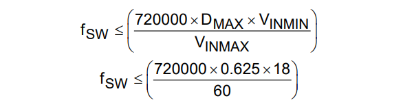
where fSW ≤ 135kHz
For this design to achieve higher efficiency, the switching frequency is selected as 125kHz. The RRT is calculated for the selected fSW:

A standard 40.2kΩ resistor is selected for RRT.
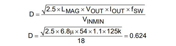
Step 3: Transformer Magnetizing Inductance and Turns Ratio
Once the switching frequency and duty cycle are selected, the transformer magnetizing inductance (LMAG) can be calculated from the energy balance equation given in the data sheet:

For the present design LMAG is chosen to be 6.8µH. The leakage inductance of the transformer should be targeted as low as possible. For this design, we have achieved leakage inductance equal to 1.7% of magnetizing inductance as follows:
LLKG = 0.017 x 6.8µ = 115.6nH
Use the following equations to calculate the maximum duty cycle of the converter for the selected frequency and magnetizing inductance:
Calculate the required transformer turns ratio (k) using the below formula:

For the present design, k is chosen as 1:1.44.
We selected the Würth Electronik transformer 750317095, which fulfills all the above mentioned required specifications for this design.
Step 4: Selection of Current-Sense Resistor
The transformer primary peak current is dependent on the output power. For the selected LMAG and fSW, the peak primary peak current is:

The value of RCS decides the peak current limit and the runaway current limit. Use the below formula to select the RCS:

For this application, a standard 6mΩ resistor is selected.
Step 5: Calculate the tONMIN and tOFFMIN
The MAX17690 has the minimum current-sense voltage threshold limit at 20mV. For the selected current sense resistor, the minimum primary peak current allowed by the converter is:

The minimum time required by the converter to reach the minimum primary peak current can be calculated as follows:

The calculated tONMIN 377.7ns is higher than the MAX17690 tONMIN constraint of 250ns. Similarly, the minimum off-time of the converter is calculated as:

The calculated tOFFMIN 604.4ns is higher than the MAX17690 tOFFMIN constraint of 500ns.
Step 6: Selection of Secondary Diode
The maximum operating reverse-voltage rating must be higher than the sum of the output voltage and the reflected input voltage.

We used a Vishay VS-10CSH02-M3 200V, 10A diode for the secondary-side rectification. This diode has a maximum 0.98V forward voltage drop.
The secondary diode forward voltage drop (VD) has a significant negative temperature coefficient. To compensate for this, a positive temperature coefficient current source is internally connected to the SET pin. The voltage at the TC pin is regulated to 0.55V at room temperature. This voltage has a 1.85mV/°C positive temperature coefficient. The RTC resistor connected between the TC pin and SGND sets the current VTC/RTC into the SET pin. δVD/δT is the temperature coefficient of the selected secondary rectifier diode and its value is 1 mV/˚C. Whereas, δVTC/δT has a value of 1.85mV/°C. Using the previous values, the RTC resistor value can be calculated to be equal to 1017.132kΩ. A typical 1020kΩ resistor is selected as RTC.
VD = 0.98V
Step 7: RRIN, RFB, and RSET Resistor Selection
Select RSET = 10kΩ. RFB and RSET are calculated as follows:

Two standard resistors of values 383kΩ and 3kΩ are used in series as RFB:
RFB1 = 383kΩ
RFB2 = 3kΩ
Note: Two series resistors are used to allow fine tuning of RFB that could be required while doing hardware testing to alleviate any parasitics effect that has not been included in the above formula. The required RRIN value can be calculated as follows:
RRIN = 0.6 x RFB = 0.6 x 386k = 231.6kΩ
A standard 232kΩ resistor is selected: RRIN = 232kΩ.
Step 8: Soft-Start Capacitor
For the desired soft-start time (tSS = 100ms), the soft-start capacitor is selected using:
CSS = 5 x tSS = 500nF
where 470nF is selected as the soft-start capacitor, CSS = 470nF.
Step 9: Selection of RVCM Resistor
Calculate the internal scaling factor KC as follows:

From Table 2 choose the next higher value for the calculated KC. For our design, the next higher value is KC = 160. Select the resistor value corresponding to the choice of KC as the RVCM, where a standard 121kΩ resistor is selected: RVCM = 121kΩ.
| KC | RVCM (kΩ) |
| 640 | 0 |
| 320 | 75 |
| 160 | 121 |
| 80 | 220 |
| 40 | Open |
Step 10: MOSFET Selection
The maximum voltage stress on the switching MOSFET during off-time is the sum of the input voltage, the reflected secondary voltage on the transformer primary, and the leakage inductance spike. The MOSFET’s absolute maximum VDS rating should be selected according to the result of the expression below:

For this application, we selected an n-channel 200V MOSFET (IPB107N20N3 G from Infineon) as the primary MOSFET.
Step 11: Output Capacitor Selection
The output capacitance is chosen so that the output voltage has at most ±3% deviation for a 50% load step of the rated output current. The bandwidth is usually selected in the fSW/20 to fSW/40 range. For the present design, the bandwidth chosen is 6.25kHz. The response time tRESPONSE and the required output capacitance can be calculated as follows:

Due to the DC-bias characteristics, a 4.7µF, 100V, 2220 capacitor offers 2.585µF at 54V. Hence, four 4.7µF, 100V, 2220 capacitors are selected for the present design.
Step 12: Loop Compensation
The MAX17690 is compensated using an external resistor capacitor network on the COMP pin. The loop compensation network are connected as shown in Figure 16. The loop compensation passive components values are calculated below. The load pole frequency is calculated as follows:


The compensation network components RZ, CZ, and CP can be calculated as follows:

A standard 4.7kΩ is selected: RZ = 4.7kΩ.

A standard 68nF capacitor is selected: CZ = 47nF.

A standard 560pF capacitor is selected: CP = 560pF.
Step 13: EN/UNLO and OVI Setting
The EN/UVLO pin serves as an enable/disable input as well as an accurate programmable input UVLO pin. The MAX17690 does not commence startup operation until the EN/UVLO pin voltage exceeds 1.215V. The MAX17690 turns off if the EN/UVLO pin voltage falls below 1.1V. A resistor-divider from VIN to SGND can be used to divide and apply a fraction of the input voltage to the EN/UVLO pin. The values of the resistor-divider can be selected so that the EN/UVLO pin voltage exceeds the 1.215V turn-on threshold at the desired input bus voltage. For an overvoltage input voltage specification of 37V and VSTART of 18V, the value of REN can be calculated as follows, assuming a 10kΩ resistor for ROVI.

A standard 24kΩ resistor is selected: REN = 24kΩ.
The same resistor-divider can be modified to implement input overvoltage protection. When the voltage at the OVI pin exceeds 1.215V, the device stops switching. The device resumes switching operations only if the voltage at the OVI pin falls below 1.1V

A standard 470kΩ resistor is selected: REN-TOP = 470kΩ.
Step 14: RCD Snubber Selection
Parasitic inductors and capacitors in the circuit, such as leakage inductance of the flyback transformer and the MOSFET output capacitance, cause voltage overshoot and ringing on the MOSFET’s drain node. Snubber circuits are used to limit the voltage overshoot to safe levels, within the voltage rating of the external MOSFET. Figure 18 shows the widely used RCD snubber circuit. Total power dissipation in the snubber can be calculated as follows:
PSNUB = 0.833 x LLK x ILIM2 x fSW
PSNUB = 0.833 x 115.6n x 12.62 x 125k = 1934mW
The RSNUB value can be calculated as follows:
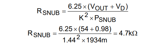
A standard 4.7kΩ is selected: RSNUB = 4.7kΩ.
The value of the CSNUB can be calculated as follows:

A standard 22nF capacitor is selected: CSNUB = 22nF.


文件和资源
-
MAXREFDES1040 Design Files2021/2/16ZIP2 M
-
MAXREFDES1040: 59.4W, No-Opto Flyback DC-DC Converter Using MAX176902021/2/16PDF1 M
支持与培训
搜索我们的知识库,获取技术问题答案。我们专门的应用工程师团队也会随时为您解答技术问题。