DC1839A

概览
产品详情
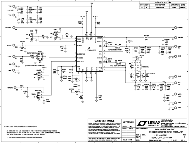
Demonstration circuit 1839A is a dual output regulator focused specifically for DDR memory power applications. It is built based on the LTC3634EFE (TSSOP-28E package), a high voltage dual channel, controlled on-time monolithic synchronous buck regulator. The DC1839A has an input voltage range of 3.6V to 15V. demo board's output voltage of the first channel, VDDQ, has three fixed voltage settings; 1.5V, 1.8V, and 2.5V, and is capable of delivering up to ±3A of output current. The second channel, VTT, is set to regulate to half the voltage on the VDDQIN pin, which can be either the channel 1 output or an external reference voltage. It can also source or sink a maximum of 3A. The LTC3634 also provides a ±10mA buffered output, VTTR, which is half of VDDQIN and is used to provide the reference voltage needed for DDR applications.
相关产品
文档
-
DC1839A - Schematic2012/3/21PDF53K
-
DC1839A - Demo Manual2011/7/22PDF180K
-
DC1839A - Design Files2011/7/22ZIP1M