Designing a Flyback Converter with the MAX17291 Micropower Boost Converter IC
Abstract
This application note discusses the designing of a low-power flyback isolated power supply using the MAX17291 for industrial applications such as the RS485 interface. The low-power isolated power supply is widely used in applications like industrial, auxiliary, or isolated power supplies.
Introduction
Flyback converters are widely used in isolated DC/DC applications because of their relative simplicity and low costs compared to alternative isolated topologies. The RS485, isolated CAN transceivers, auxiliary power supplies, etc. are a few applications of the low-power flyback topology. A flyback converter can be designed using a MAX17291 boost converter with a 3.75kV isolation.
The MAX17291 is a low-quiescent current boost (step-up) DC-DC converter with a 1A peak inductor current limit and True Shutdown™. The True Shutdown disconnects the output from the input with no forward or reverse current. The out¬put voltage is set with an external resistor-divider. The MAX17291 is a highly integrated boost converter designed for applications requiring high voltage and tiny solution size, such as sensor modules. It in¬tegrates a power switch, power diode, and output load switch.
| Features | Performance |
|
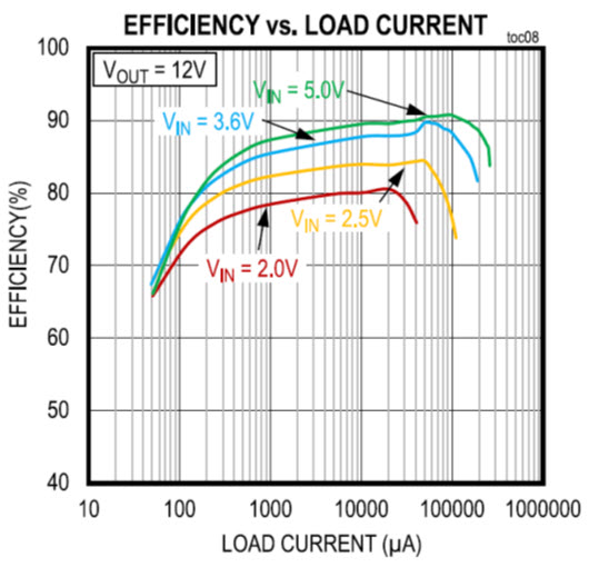
Figure 1. Efficiency graph. |
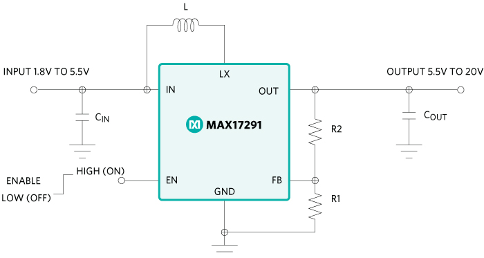
Figure 2. Application circuit of the MAX17291 boost converter.
| Parameter | Value |
| Input Voltage | 4.5V to 5.5V |
| Output Voltage | 5.0V |
| Output Current | 300mA Maximum |
| Isolation Voltage | 3.75kV (IEC 60950-1, Reinforced Insulation) |
Operation of a Flyback Converter
The operating principle of a flyback converter is like a buck-boost converter, but with an additional transformer to achieve galvanic isolation. The output voltage can be adjusted by varying the turns ratio of the transformer. Figure 3 illustrates a typical flyback converter.
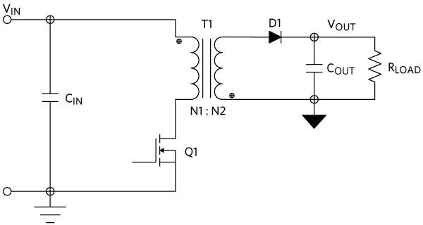
Figure 3. Flyback converter.
The operation of a flyback converter is explained in two states.
Switch Q1 ON
The input voltage appears across the primary of the transformer when the switch Q1 is ON and the current starts flowing through the primary of the transformer. The polarity of the transformer windings is in such a way that a negative voltage appears at the anode of the output diode. It becomes reverse-biased and blocks the current flow through the secondary circuit during this state.
Thus, the whole energy is stored in the primary inductance rather than transferring the energy to the secondary. Hence, this transformer is a coupled inductor.
The increase in the inductor current when Q1 is ON is calculated as:
VL = VIN = L × ?IL /?T
?IL = VIN × TON/L
?IL = VIN × D × TS /L … (1)
where:
- ?IL is the change in the inductor current
- VIN is the input voltage
- TS is the switching time
- D is the duty cycle
- L is the primary inductance of the transformer
The output capacitor, in the steady-state operation, supplies current to the load when the switch Q1 is on.
Switch Q1 OFF
The polarity across the primary winding reverses at the end of the ON time when the switch Q1 becomes OFF, and hence the polarity on the secondary winding also reverses. The energy stored in the primary is transferred to the secondary side. The diode D1 starts conducting and current flows to output capacitor COUT and load. The inductor current decreases during this time and is given as:
?IL = VOUT × N1/N2 × TOFF/L
?IL = VOUT × N1/N2 × (1 - D) × TS /L … (2)
The voltage across Q1 is equal to the input voltage, reflected voltage of the secondary and leakage inductance voltage during Q1 OFF time.
VQ1 = VIN + N1/N2 × VOUT + VLEAK … (3)
where VLEAK is the voltage due to leakage inductance.
The inductor current change over one switching cycle must be equal to zero during the steady-state operation and the output voltage is given as:
VOUT = D/1-D × N2/N1× VIN
D = VOUT / VOUT + (N2/N1) × VIN … (4)
The MAX17291 is a boost converter IC. It has an internal MOSFET and control circuit. Figure 4 illustrates the flyback converter using the MAX17291 IC.
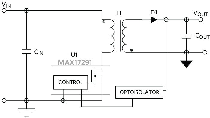
Figure 4. Flyback converter using the MAX17291.
Transformer Design
The MOSFET for this design is inside the IC. The reflected voltage from the secondary side is used to design the transformer. The drain to source voltage rating of the MOSFET in the MAX17291 IC is 20V. When the MOSFET Q1 is off, the voltage across MOSFET Q1 is given by equation 3.
VDS = VIN + VREF + VLEAK
The reflected voltage across the primary winding due to the secondary is:
VREF = 0.8 × VDS - VIN - VLEAK
VREF = 0.8 × 20 - 5 – 5 = 6V… (5)
where:
- VREF is the reflected voltage across the primary winding.
- VDS is the maximum drain to source voltage rating of the MOSFET.
- VIN is the input voltage.
- VLEAK is the voltage spike due to leakage inductance.
The turns ratio of the transformer is calculated as:
VREF = (VOUT + VF ) × N1/N2
where:
- VOUT is the output voltage.
- VF is the diode forward drop.
- N1/N2 is the transformer turns ratio.
N1/N2 = VREF/VOUT + VF = 6/5 + 0.5 = 1.09 … (6)
The duty cycle of the flyback converter is calculated from the VOUT expression of equation 4.
D = 5 + 0.5/(5 + 0.5) + 1.09 × 4.5 = 0.55… (7)
The peak current limit of MAX17291 IC is 1A, and considering the current ripple as 50% of the inductor peak current, the maximum output current is calculated as:
IIN = ILPK - ILPK - PK/2 = IOUT /(1 – D) × N2/N1… (8)
The MAX17291 IC operates in the fixed OFF time in the CCM mode of operation at 1MHz switching frequency. The OFF time is calculated based on the input voltage and the voltage on OUT pin of the IC, which is the output voltage of the boost converter. The OFF time is inversely proportional to VOUT . So, a dummy resistor is needed across the OUT pin and ground to maintain the voltage within range, and the switching frequency within 1Mz to 1.5MHz.
The inductance value of the transformer is calculated as:
L = VIN × D × TS /?IL = 4.5 × 0.55/0.5 × 1 × 10-6 = 4.95µH … (9)
An optocoupler and TL431 circuit are used for the output voltage feedback sensing and control for tighter output voltage regulation. They are also used to achieve the isolation between the primary and secondary circuit. According to the output voltage measured, the optocoupler drives the FB pin of the IC and regulates the output voltage with the load and line changes. Figure 5 shows the schematic of the MAX17291 flyback converter with the optocoupler feedback.
Selecting the Diode
The diode is forward-biased and the output current flows through the diode to the output capacitor and load during the Q2 off time. The maximum output current for this design is 300mA.
The diode in the secondary side is reverse-biased during Q1 ON time. The maximum voltage across the diode appears at maximum input voltage condition and is given as:
VD = VOUT + N2/N1 × VIN
VD = 5 + 1.09 × 5.5 = 10.995V
So, select a diode with reverse voltage rating of more than 10.5V and average current rating of around 1A. Choose a Schottky diode that dissipates less power during high-frequency operation as the converter is switching at high frequency and operating in the CCM mode from medium loads to full load.
Schematic of the Flyback Converter
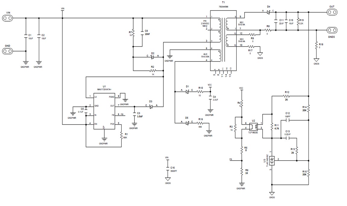
Figure 5. Flyback converter schematic using the MAX17291.
Flyback Converter Test Data
| VIN (V) | IIN (mA) | VOUT (V) | IOUT (mA) | VOUT ERR (%) | EFF (%) |
| 5.0 | 26.6 | 5.07 | No-load | 1.4 | - |
| 5.0 | 35.4 | 5.07 | 5.1 | 1.4 | 14.5 |
| 5.0 | 64.5 | 5.07 | 25.0 | 1.4 | 39.3 |
| 5.0 | 97.3 | 5.07 | 50.4 | 1.4 | 52.5 |
| 5.0 | 129.8 | 5.06 | 75.3 | 1.3 | 58.8 |
| 5.0 | 161.6 | 5.06 | 100.2 | 1.3 | 62.8 |
| 5.0 | 228.6 | 5.06 | 150.5 | 1.3 | 66.7 |
| 5.0 | 300.8 | 5.07 | 200.8 | 1.3 | 67.6 |
| 5.0 | 378.9 | 5.07 | 250.5 | 1.3 | 66.9 |
| 5.0 | 464.3 | 5.07 | 301.1 | 1.3 | 65.7 |
Efficiency Plot
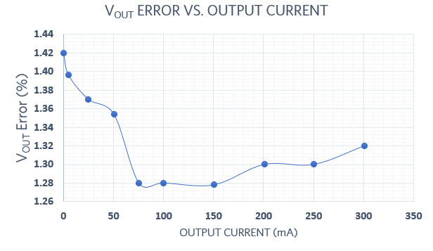
Figure 6. Efficiency plot at VIN = 5V, VOUT = 5V.
Load Regulation Plot
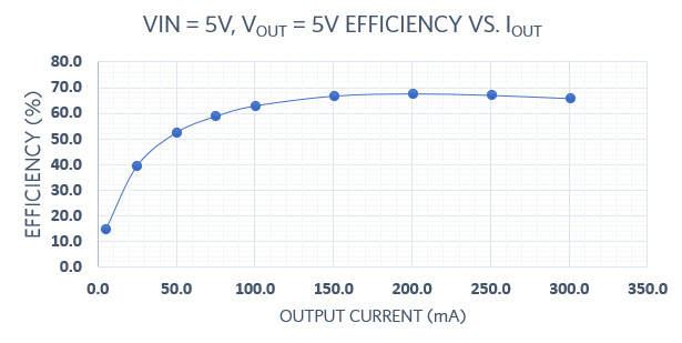
Figure 7. Load regulation plot at VIN = 5V, VOUT = 5V, IOUT = 300mA.
Steady-State Waveforms: VIN = 5V, VOUT = 5V, IOUT = 300mA
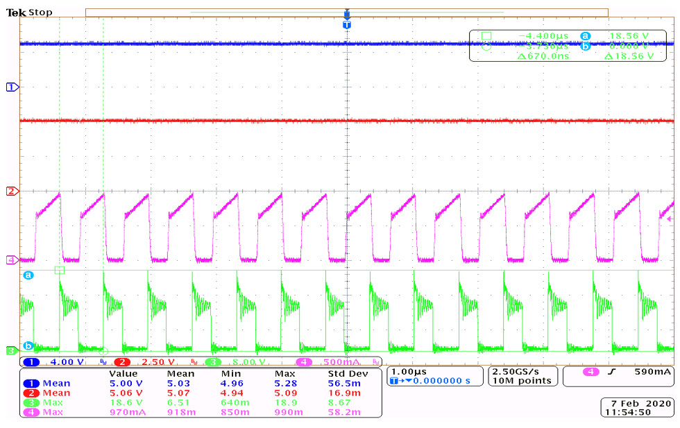
Figure 8. Steady-state operation at VIN = 5V, VOUT = 5V, IOUT = 300mA.
Load Transient: VIN = 5V, VOUT = 5V, , IOUT = 1 to 300mA
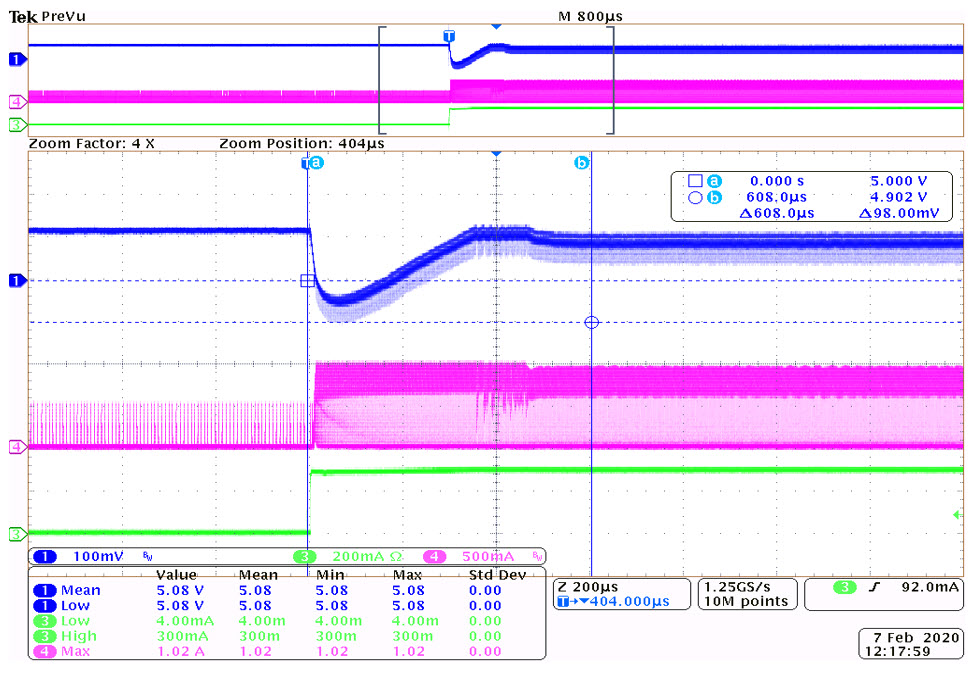
Figure 9. Load transient at VIN = 5V, VOUT = 5V, IOUT = 1 to 300mA.
The VOUT drop is 98mV (1.96%).
The settling time is 608us.
Output Voltage Ripple: VIN = 5V, VOUT = 5V, IOUT = 300mA
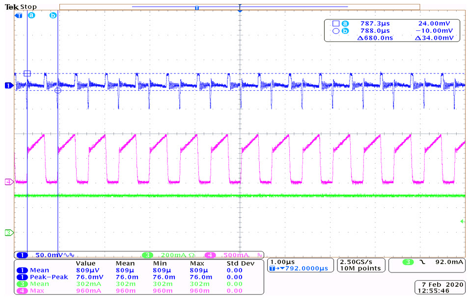
Figure 10. Output voltage ripple at VIN = 5V, VOUT = 5V, IOUT = 300mA.
The output voltage ripple is 76mV (1.52%).
| Item | REF DES | QTY | Description |
| 1 | C1, C2 | 2 | 10uF 10% 10V X7R ceramic capacitor (0805) Murata GRM21BR71A106KA73 |
| 2 | C3 | 1 | 1uF 10% 25V X7R ceramic capacitor (0805) Samsung CL21B105KAFNNNE |
| 3 | C4 | 1 | 2.2uF 10% 25V X7R ceramic capacitor (0805) Samsung CL21B225KAFNNNE |
| 4 | C5 | 1 | 0.1uF 10% 25V X7R ceramic capacitor (0805) Murata GRM188R71E104KA01 |
| 5 | C8 | 1 | 10nF 10% 25V X7R ceramic capacitor (1206) Kemet C1206C103K5RACTU |
| 6 | C11, C15 | 1 | 10uF 10% 16V X7R ceramic capacitor (0805) Samsung CL21B106KOQNNNE |
| 7 | C13 | 1 | 0.22uF 10% 50V X7R ceramic capacitor (0805) Murata GRM21BR71H224KA01 |
| 9 | C16 | 1 | 3300pF 10% 250V X7R ceramic capacitor (2220) Vishay VJ2220Y332KXUSTX1 |
| 10 | D1 | 1 | 30V 200mA Small Signal Schottky diode (SOD-323) BAT54H |
| 11 | D2, D4 | 2 | 100V 1A Schottky diode SMB B1100LB-13-F |
| 12 | R1 | 1 | 100kO 1% resistors (0805) |
| 13 | R11 | 1 | 4.7kO 1% resistors (0805) |
| 14 | R4, R8, R18, R5 | 4 | 0O 1% resistors (0805) |
| 15 | R6 | 1 | 1kO 1% resistors (0805) |
| 16 | R7 | 1 | 1kO 1% resistors (2512) |
| 17 | R10 | 1 | 10O 1% resistors (0805) |
| 18 | R12-R13 | 2 | 2kO 1% resistors (0805) |
| 19 | R14-R15 | 2 | 20KO 1% resistors (0805) |
| 20 | T1 | 1 | TRANSFORMER; 1:1; PRI: 2.5-5V; 1MHZ; 750344566 |
| 21 | U1 | 1 | MAX17291ATA+ TDFN8-EP |
| 22 | U2 | 1 | TLP185(SE) IC PHOTOCOUPLERS SO6-4 |
| 23 | U3 | 1 | TL431AIDBZ IC; PRECISION PROGRAMMABLE REFERENCE; SOT23-3 |
Conclusion
This application note discusses the steps to design an isolated flyback converter using the MAX17291 integrated boost converter IC. It also discusses the component selection and transformer designing procedure.
