Using Multiple DS1267 Digital Potentiometers With an 8051 Microprocessor Generating 3-Wire Signals
Abstract
The DS1267 is a dual digital potentiometer with a serial \"shift register\" type interface. The shift register has an input pin where data is shifted in as well as an output pin which shifts data out of the last bit of the shift register when being written. This allows multiple DS1267s to be daisy-chained together and programmed together on the same serial bus. The application note describes how to accomplish this with circuit examples and pseudo code examples showing how to develop the code for any microprocessor.
Introduction
Dallas Semiconductor's DS1267 Digital Potentiometers are ideal for systems requiring Digital to Analog Converters (DAC), or systems that need a programmable bias current, voltage, or resistance without the human intervention required by a traditional mechanical potentiometers. The DS1267 provides two digital potentiometers in one package. A unique 3-wire protocol allows several of these chips to be placed in series or in parallel. An optional stacked configuration allows the chip's two 8-bit potentiometers to be placed in series, providing 9-bit accuracy. The DS1267 can be used in dual supply systems with an input range between -5V and +5V as long as the substrate bias voltage is below the lowest input voltage used.
This application note provides an overview of different configurations for communicating to multiple DS1267s with a common bus. It also provides the hardware and software required for communicating to two DS1267s daisy-chained together in a series.
Hardware Setups for Communication with a DS1267
There are two primary ways that a 3-Wire bus can be connected to communicate with multiple chips. The devices can either be connected in series, or in parallel. For either type of connection, 17 bit blocks of data will be written to the part(s) at a time. The data will determine the position of the potentiometer wipers and the stack output each time that the reset is de-asserted.
Series
A standard series connection is shown in Figure 1 below. This method of connection works with microprocessors that have bidirectional ports that are high impedance when expecting input. This allows the feedback resistor to be used to drive the DQ pin from the COUT of the last device in the daisy chain. If it is not desirable to read from the part, then the isolation resistor can be omitted. This method allows an indefinite number of chips to be placed in series.

Figure 1. Three DS1267s Connected in Series with a Feedback Resistor for Reading the Shift Register.
Note: The feedback resistor should be approximately 10kΩ to provide adequate isolation between I/O pin-2 and COUT when I/O pin-2 is driving DQ.
The second method of serial connection (Figure 2) must be used for microprocessors that have open-collector I/O ports. On an open collector port, there is either an internal (true of the 8051 microprocessor) or external pull-up resistor that allows a high signal to be produced without a high side driver. This is typically done to eliminate the possibility that the microprocessor will be in contention with some external device connected to it. If an isolation resistor were connected between COUT and DQ as shown in Figure 1, then it would cause errors during write cycles to the part whenever COUT is attempting to drive the DQ pin low, because COUT will out-drive the weak pull-up resistor. The setup shown in Figure 2 allows the shift register in the DS1267 to be read using one additional pin for input only on an open collector port. Typical 3-wire signals control the DS1267 as before.
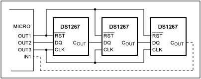
Figure 2. Series Connection of DS1267s with a Separate Input Used to Read from the Shift Register.
In both series connection cases, the feedback from the DS1267 can be omitted, and it will only require three wires to write to as many DS1267s as desired. If the status of the potentiometer must be known at a later time, 2 bytes of RAM will have to be devoted to keep track of the values written to each DS1267 attached to the bus. The main downfall of the series method is that n DS1267s on serial bus take n times as long to write to or read from as a single chip does.
Parallel
The second class of setup is a parallel configuration. Figure 3 shows a parallel setup that can be used to write to several DS1267s with DQ and CLK in common and separate RST signals. The advantage of this system is that it requires only 17 DS1267 clock cycles to write to any part being used. The disadvantage is that it requires one additional output pin per additional DS1267. If several DS1267s and high-speed writing are required, it would be possible to decode an address to produce the reset (chip select) signals with the addition of a decoder. This would allow the operation of 2(# of select pins available) DS1267s. Thus, if you had three I/O pins available to decode address, then you could decode them to allow eight DS1267 dual potentiometers (16 potentiometers in eight packages) to operate with common DQ and CLK signals. If a decoder was used for the system below, then five more potentiometers could be added without loss of another output pin.

Figure 3. Three Parallel Configured DS1267s Sharing Common DQ and CLK Lines.
The setup above does not incorporate any provisions for reading from the DS1267s. If the potentiometers are to be read in a system using a decoder, then the decoders address lines could be used with a mux to read all of the COUTs into either a single bidirectional I/O pin or a separate input pin as before.
The hardware setup shown in Figure 4 (next page) was used to generate the code in Appendix A. Providing a 22.2 MHz clock for the DS87C520 microprocessor. A DS232A converts the 5V CMOS signals to RS232 levels for communication between the microprocessor and PC. The DS232A is connected to a standard serial port plug, which can be connected to a PC to allow feed back from the microprocessor at 19200 baud (1 stop bit, no parity, no flow control). The two potentiometers are daisy-chained (connected in series), and connected to the microprocessor on port 1. The first DS1267 is connected in the stacked configuration, and is providing a 9-bit DAC. The second DS1267 is providing two 8-bit DACs. Because they are connected in series, each read and write attempt will involve shifting 2*17 bits. An LED has also been connected to port 1.0 as a status indicator.
Note: The 8051 has open-collector ports; therefore, a separate input pin must be used for COUT. Using DQ as a bidirectional port pin will cause communication errors between the microprocessor and the DS1267s. Also, if the serial port is to be used, the clock rate must be near 22.118 MHz. Failure to have a clock rate within 2-3% of that frequency can cause serial port communication errors.

Figure 4. DS87C520 Microprocessor DS232A Serial Port Transmitter, and Two DS1267s Daisy-Chained on a 3-Wire Bus.
3-Wire Protocol
The 3-wire protocol is a simple protocol to program the DS1267's two potentiometers via a 17-bit shift register. The shift register is controlled with the reset, data, and clock signals. Reset (RST) is used to select the chip. This signal is active high, and must be asserted during any attempt to write to or read from the part. The data pin (DQ) is used to transfer data to the part. Once the data is correctly placed on DQ, the clock signal (CLK) is pulsed to synchronize the data transfer. The timing for these events is shown in the DS1267 data sheet. Data that is shifted into the part can continue being shifted through to another 3-wire device with the cascade output (COUT.) The cascade output can also be routed back to the controller to allow a microprocessor to read what it has written.
The data format for two devices connected in series is shown in Figure 5.

Figure 5. Two 17-Bit DS1267 shift registers cascaded together for series operation.
In this configuration, the first bit shifted into the register is shifted all the way to the end. Thus, the first bit that is placed on DQ at the beginning of data transfer would be STK#2. This is the stack control bit for DS1267 #2. The next 8-bits that will be sent are the 8-bits that control the position of wiper 1, on DS1267 #2, labeled potentiometer 3 on the diagram. Notice that the MSB of the byte is sent to the part first. Then the next 8-bits will control potentiometer 2. The next bit sent will be STK#1, which controls the stack output of DS1267 #1. The bytes for Potentiometers 1 and 0 will follow the stack control bit respectively. If only one chip were connected on the bus, then only 17-bits of data would be communicated to the part, but the data would be in the same format as shown in the first half of Figure 5.
To write the 17 bits out to one of the DS1267s, the following procedure must be performed:
- Assert RST (high)
- Place a data bit on DQ pin
- Pulse CLK
- Repeat steps 2) and 3) 16 more times
- De-assert RST (low)
If n DS1267s are cascaded together, then steps 2) and 3) are performed n × 17 times before RST is deasserted.
If the optional feedback resistor has been used with bi-directional port, the values stored in the shift register are read by accomplishing the following:
- Assert RST, and place I/O pin-2 in a high impedance state.
- Read I/O pin-2 (equal to COUT if I/O pin-2 is in a high impedance state).
- Pulse CLK.
- Repeat steps 2) and 3) 16-times more times.
- De-assert RST.
To read from the part that is has COUT connected to a separate input, the following sequence must be completed:
- Assert RST.
- Read COUT at the input pin.
- Write value of COUT to DQ.
- Pulse CLK.
- Repeat 2), 3), and 4) 16 more times.
- De-assert RST.
Note: The value of COUT must be written back to DQ, because there is no difference in the operation of the reset and clock signals between a read and a write attempt. Thus, COUT is being written back into DQ as was done by the hardware in figure 1. Also, if n DS1267s are attached in series, then sequences 2, 3, and 4 must be performed n × 17 times, or the DS1267s will not have the same data in them as when the read routine was begun.
Controlling Two DS1267s Using Software Generated 3-Wire Communication
Main 3-Wire Communication Routines
The method of communicating to the DS1267 described in the 3-Wire Protocol section is accomplished in code by four routines. These routines are used to write 34 bits, read 34 bits, serialize the bytes of data to be sent to each potentiometer, and reconstruct the bits of data received from the potentiometer into bytes. The former two routines call the later two respectively. The code is located in Appendix A, and brief descriptions of these routines are listed below.
WritePots3
This routine is the master writing routine. It writes the stack control bits stored in the memory locations called stack1 and stack2, and it writes out all of the data to the potentiometers with the WriteBits3 routine. The data that is to be written out to the DS1267s is stored in 4 bytes (PotData0, PotData1, PotData2, and PotData3).
WriteBits3
This routine writes the byte stored in the accumulator by rotating the MSB into the carry bit, writing the carry bit to DQ, and finally pulsing CLK. This is repeated a total of eight times, which writes the entire byte to the DS1267.
ReadPots3
This routine is the master reading routine. It reads the stack control bits and stores them in the memory locations called stack1 and stack2. It also uses the ReadBits3 routine to read back the 8-bits of information controlling each potentiometer and stores the values in the 4-bytes labeled PotData0, PotData1, PotData2, and PotData3
ReadBits3
This routine reads the 8-bits back from the potentiometer used to store the wiper positions, converts the 8- bits into a byte, and passes the data back to the calling procedure in the accumulator.
Other Routines
These routines each support the main communication routines by performing the function described below.
initSP1
Initializes serial port 1.
intro
Displays a welcome message on the PC terminal via serial port 1
init3wire
Initializes the 3-Wire Bus signals (RST, DQ, CLK), and sets the values in the variables used write to the potentiometers (stack1, stack2, PotData0, PotData1, PotData2, PotData3
wt
Programmable wait function. Uses wait16us, and registers R5, R6 and R7 to realize a delay between 14.42 µs and 3.7 min.
wait16us
Delays 1.6 µs each time called.
DisplayPots:
Uses outchar and binasc to display the values read back from each potentiometer. It is not required code for the operation of the DS1267s, but it makes it a lot easier to debug reading problems when you can verify the data in the storage bytes is correct after a read attempt.
outchar
Places a single character into the serial port 1 buffer, then waits for the serial transmission complete flag to be set before returning.
binasc
Converts an integer stored in the accumulator into two ASCII bytes in hexadecimal format.
outstr
Uses outchar to send null terminated strings to the PC via serial port 1. The strings sent are stored in the message section at the very end of the code.
Main Program
The main program performs the following sequence:
- Disables interrupts
- Initializes serial port 1
- Initializes 3-wire pins and variables
- Inverts an LED located on P1.0 to signify the beginning of the program
- Writes the potentiometers to the values stored during initialization
- Delays 5 seconds, this is done so a multimeter can be used to determine if a read function (next) is over-writing the potentiometers to different values
- Reads the potentiometers
- Displays the results
- Begins blinking the LED, once per second to signify that the program has finished execution
Appendix A–Code Used to Generate 3-Wire for the DS1267 Using a DS87C520 Microprocessor
;*********************************************************************
;* DS87C520 APPS DEVELOMENT SYSTEM *
;* *
;* Application: Communication with a DS1267, and a PC via *
;* Serial Port 1. *
;*********************************************************************
;* *
;* This program was created to demonstrate using a 3-Wire interface *
;* to communicate with a DS1267 Digital Potentiometer. The program *
;* also talks to PC via Serial Port 1 (19200 Baud). The micro is *
;* operated using DS1077 Oscillator operating at 22.2MHz. *
;* *
;* Software Revision History *
;* *
;* 1.0 01/19/01 - First try at operating a DS1267 using the *
;* generic application engineering generic 8051 *
;* boot loading board. *
;* *
;* Hardware Description *
;* *
;* P1.0 - LED P0.0 - SN74F373N *
;* P1.1 - P0.1 - " *
;* P1.2 - RXD1 - PC P0.2 - " *
;* P1.3 - TXD1 - PC P0.3 - " *
;* P1.4 - CLK P0.4 - " *
;* P1.5 - DQ P0.5 - " *
;* P1.6 - RST P0.6 - " *
;* P1.7 - COUT P0.7 - " *
;* *
;* P3.0 - RXD0 - Not used P2.0 - Upper *
;* P3.1 - TXD0 - Not used P2.1 - Address *
;* P3.2 - P2.2 - Byte *
;* P3.3 - P2.3 - " *
;* P3.4 - P2.4 - " *
;* P3.5 - P2.5 - " *
;* P3.6 - WR\ P2.6 - " *
;* P3.7 - RD\ P2.7 - " *
;* *
;* Window 0 R0 - Used for 3-wire read and write, Do not destroy!; *
;* Window 0 R1 - Used for binasc routine, Do not destroy!; *
;* Window 0 R5-R7 Used for timer/scratch pad, destroy with caution!; *
;*********************************************************************
$include (c:\firmware\reg520.inc) ; SFR register defs for compiler

;************* Variable Declarations *************
;** General Variables **
stack equ 02Fh ; bottom of stack
; stack starts at 30h
;** DS1267 Variables **
stack1 bit 000h ; Read DS1276#1 Stacked?
PotData0 equ 042h ; Write Data DS1267#1, pot0
PotData1 equ 043h ; Write Data DS1267#1, pot1
stack2 bit 001h ; Read DS1267#2 Stacked?
PotData2 equ 044h ; Write Data DS1267#2, pot0
PotData3 equ 045h ; Write Data DS1267#2, pot1

;************* SFR Declarations *************
;** General SFR Names **
smod_1 equ 0DFh ; baud rate doubler bit declared
;** Port 1 Signal Names **
LED equ 90h ; P1.0 is LED
; P1.1 is not used
RX1 equ 92h ; P1.2 is Serial Port 1 RX
TX1 equ 93h ; P1.3 is Serial Port 1 TX
CLK equ 94h ; P1.4 is CLK - 3Wire
DQ equ 95h ; P1.5 is DQ - 3Wire
RST equ 96h ; P1.6 is RST - 3Wire
COUT equ 97h ; P1.7 is COUT - 3Wire

;*********************************************************************
;* Hardware Interrupt Vectors (Table on page 95 of DS databook) *
;*********************************************************************
;* No Interrupts are enabled in this code. If interrupts are to be *
;* enabled they need to have the label initialized here. *
;*********************************************************************

org 0000h ; Power up and Reset
ljmp start
org 0003h ; External Interrupt 0
ljmp start
org 000Bh ; Timer 0 Interrupt
ljmp start
org 0013h ; External Interrupt 1
ljmp start
org 001Bh ; Timer 1 Interrupt
ljmp start
org 0023h ; Serial Port 0 Interrupt
ljmp start
org 002Bh ; Timer 2 Interrupt
ljmp start
org 0033h ; PowerFail Interrupt (DS Priority 1)
ljmp start
org 003Bh ; Serial Port 1 Interrupt (DALLAS)
ljmp start
org 0043h ; External Interrupt 2 (DALLAS)
ljmp start
org 004Bh ; External Interrupt 3 (DALLAS)
ljmp start
org 0053h ; External Interrupt 4 (DALLAS)
ljmp start
org 005Bh ; External Interrupt 5 (DALLAS)
ljmp start
org 0063h ; Watchdog Interrupt (DALLAS)
ljmp start
org 006Bh ; Real-Time Clock (DALLAS)
ljmp start

;*********************************************************************
;**** Main Program ****
;**** This program talks to two DS1267s using 3-wire. It also ****
;**** demonstrates reading from the DS1267s using a 4th pin as ****
;**** an input from the Cout of the last DS1267. ****
;*********************************************************************

org 0080h;
start:
clr EA ; Disable Interrupts
lcall initSP1 ; Initialize Ser Port 1 & Timer 1/0
lcall intro ; Welcome Message, Serial Port 1
lcall init3wire ; Initialize 3-wire Variables
cpl LED ; Complement LED9 - Identifies that the
; has started execution
lcall WritePots3 ; write to the pots - writes the values
; stored in the RAM locations by init3wire
mov R5, #255 ; set timer up for a 5.0 second delay
mov R6, #147 ; "
mov R7, #10 ; "
lcall wt ; call timer function
lcall ReadPots3 ; read data from pots, re-write the data
; back to the part.
lcall DisplayPots3 ; display the data from the DS1267s
endmain:
mov R5, #255
mov R6, #147 ; R5=255,R6=147 => R7 * 0.5 Sec
mov R7, #1 ; 0.5 Sec Delay
lcall wt
cpl LED ; Blink LED once per second
sjmp endmain ; Waits forever

;*********************************************************************
;**** 3-Wire Write Pots Routine for DS1267s ****
;**** Writes the 34 bits out to the two DS1267s ****
;*********************************************************************
;* requires WriteBits3 routine *
;* WriteBits3 destroys the R0 and A registers *
;*********************************************************************

WritePots3:
setb RST ; set RST to begin data xfer
mov C, stack2 ; set 1267#2 stack condition=stack2
mov DQ, C
setb CLK ; clock 3-wire bus
clr CLK ;
mov A, PotData3 ; moves PotData3 into A for xmission
lcall WriteBits3 ; call WriteBits3 to write serial byte
; out to the DS1267s
mov A, PotData2 ; moves PotData2 into A for xmission
lcall WriteBits3 ; call WriteBits3 to write serial byte
; out to the DS1267s
mov C, stack1 ; set 1267#1 stack condition=stack1
mov DQ, C ;
setb CLK ; clock 3-wire bus
clr CLK ;
mov A, PotData1 ; moves PotData1 into A for xmission
lcall WriteBits3 ; call WriteBits3 to write serial byte
; out to the DS1267s
mov A, PotData0 ; moves PotData0 into A for xmission
lcall WriteBits3 ; call WriteBits3 to write serial byte
; out to the DS1267s
clr RST ; clear RST to end data XFER
ret

;*********************************************************************
;**** 3-Wire Write Bits Routine for DS1267s ****
;**** Writes 8 bits by toggling the DQ and the CLK pins as ****
;**** required. This is used to write 8-bit potentiometer ****
;**** values out to the parts ****
;*********************************************************************
;* requires no other routines, destroys R0 and A registers *
;*********************************************************************

WriteBits3:
mov R0, #8 ; 8-bits in transfer
WBit3:
rlc A ; rotate MSB to carry bit
mov DQ, C ; mov C onto DQ pin
setb CLK ; clock 3-wire bus
clr CLK ;
djnz R0, WBit3 ; if all 8-bits not send, keep sending
ret ; else return

;*********************************************************************
;**** 3-Wire Read Pot Routine for DS1267s ****
;**** Reads 34 bits of information from the DS1267 by using ****
;**** ReadBits3 and by toggling the RST, DQ and the CLK pins ****
;**** to read the Stack Bits as required. ****
;*********************************************************************
;* requires readbits3 routine *
;* readbits3 destroys R0 and A *
;*********************************************************************

ReadPots3:
clr PotData0 ; Clear PotDataX registers to guarantee the
clr PotData1 ; values displayed are not the values
clr PotData2 ; left in the registers from programming
clr PotData3 ; the DS1267s
setb RST
mov C, COUT ; Copy COUT into C
mov DQ, C ; Wrap the contents back out onto DQ..
; ..so the DS1267s will still have the same
; values after the read attempt
mov stack2, C ; copy C into stack2
setb CLK ; clock DS1267s
clr CLK ;
lcall ReadBits3 ; read next byte
mov PotData3, A ; mov Data to Storage Byte
lcall ReadBits3 ; read next byte
mov PotData2, A ; mov Data to Storage Byte
mov C, COUT ; Copy COUT into C
mov DQ, C ; Wrap Data back into part
mov stack1, C ; copy C into stack1
setb CLK ; clock DS1267
clr CLK ;
lcall ReadBits3 ; read next byte
mov PotData1, A ; mov Data to Storage Byte
lcall ReadBits3 ; read next byte
mov PotData0, A ; mov Data to Storage Byte
clr RST
ret

;*********************************************************************
;**** 3-Wire Read Bits Routine for DS1267s ****
;**** Reads 8 bits by toggling the DQ and the CLK pins as ****
;**** required. This is used to read the 8-bit potentiometer ****
;**** values from the parts ****
;*********************************************************************
;* requires no other routines *
;* destroys R0 and A registers *
;*********************************************************************

ReadBits3:
mov R0, #8 ; 8-bits in transfer
RBit3:
mov C, COUT ; mov COUT into C
mov DQ, C ; Write COUT onto DQ - Wrap Data back into part
rlc A ; rotate carry bit to MSB of A
setb CLK ; clock 3-wire bus
clr CLK ;
djnz R0, RBit3 ; if all 8-bits not send, keep sending
ret ; else return

;*********************************************************************
;**** Display DS1267 Pots Routine ****
;**** Displays the value of the registers used for all 4 ****
;**** Digital Potentiometers using serial port 1 ****
;*********************************************************************
;* requires binasc and outchar, outstr routines *
;*********************************************************************

DisplayPots3:
jb stack1, stkd1 ; if not stacked then write "N "
mov A, #'N'
lcall outchar
mov A, #' '
lcall outchar
sjmp next1
stkd1:
mov A, #'S' ; else write "S "
lcall outchar
mov A, #' '
lcall outchar
next1:
mov A, PotData0 ; move data read from RAM @PotData0 to A
lcall binasc ; convert data from bin to ascii
lcall outchar ; send first byte via Ser. Port1
mov A, R1 ; mov 2nd conversion byte from R1>A
lcall outchar ; send second byte via Ser. Port1
mov A, #' ' ; send Space via Ser. Port1
lcall outchar
mov A, PotData1 ; Move data read from RAM @PotData1 to A
lcall binasc ; convert data from bin to ascii
lcall outchar ; send first byte via Ser. Port1
mov A, R1 ; mov 2nd conversion byte from R1>A
lcall outchar ; send second byte via Ser. Port1
mov A, #' ' ; send Space via Ser. Port1
lcall outchar
jb stack2, stkd2 ; if not stacked then write "N "
mov A, #'N'
lcall outchar
mov A, #' '
lcall outchar
sjmp next2
stkd2:
mov A, #'S' ; else write "S "
lcall outchar
mov A, #' '
lcall outchar
next2:
mov A, PotData2 ; Move data read from RAM @PotData2 to A
lcall binasc ; convert data from bin to ascii
lcall outchar ; send first byte via Ser. Port1
mov A, R1 ; mov 2nd conversion byte from R1>A
lcall outchar ; send second byte via Ser. Port1
mov A, #' ' ; send Space via Ser. Port1
lcall outchar
mov A, PotData3 ; Move data read from RAM @PotData3 to A
lcall binasc ; convert data from bin to ascii
lcall outchar ; send first byte via Ser. Port1
mov A, R1 ; mov 2nd conversion byte from R1>A
lcall outchar ; send second byte via Ser. Port1
mov DPTR, #mess2 ; send (2)LF and (2)CR via Ser. Port1
lcall outstr ;
ret

;*********************************************************************
;**** 3-Wire Init Routine for DS1267 ****
;**** Initializes 3 wire pin values ****
;*********************************************************************
;* requires no additional routines *
;* destroys no registers *
;*********************************************************************

init3wire:
clr RST ; clear reset pin
clr CLK ; clear clock pin
clr DQ ; clear data pin
mov PotData0, #0CDh ; set #1, Sout to 2V, 205d if not stack1
mov PotData1, #99h ; set #1, Sout to 4V, 153d if stack1
setb stack1 ; set #1, stack on, set SOUT to 4V
mov PotData2, #66h ; set #2, pot0 to 2V, 102d
mov PotData3, #99h ; set #2, pot1 to 3V, 153d
setb stack2 ; set #2, stack on
ret

;*********************************************************************
;**** Wait 1.6 us Function
****
;**** Wastes 1.6us of processor time with call, nop and return ****
;*********************************************************************
;* Requires no other routines or registers *
;*********************************************************************
wait16us:
nop ; 1 nops @4cc each + lcall @16cc + ret @16cc
; produces approximately 1.6us of delay with a
; 22.22MHz clock
ret

;*********************************************************************
;**** Initialize Serial Port 1 for PC interface ****
;**** Set up serial port 1 for use with a 22.1 MHz crystal ****
;**** Uses timer 1 for 19200 baud, Mode 1 ****
;*********************************************************************
;* Uses no other routines or registers *
;*********************************************************************

initSP1:
setb smod_1 ;enable baud rate doubler
mov SCON1, #50h ;Serial Port 0 asynch, 10 bits
mov TMOD,#21H ;MSB-T1 on and in 8bit auto-load-mode
;LSB-T0 on and in 16-bit count mode
; T0 is free running 2^16cc
; overflow rate (35.59ms)
mov TCON, #50H ;t1/0 enabled, not using ext int
; edge/level select and detect
; flag/reg
mov TH1, #0FAH ;set t1 reset val / baud rate=19200
ret

;*********************************************************************
;**** Intro Display Message Routine ****
;**** Sends out a greeting message ****
;*********************************************************************
;* Uses outstr function *
;* Destroys DPTR *
;*********************************************************************

intro: mov DPTR, #mess1 ;send welcome message
lcall outstr
mov DPTR, #mess2 ;send (2) CR and (2) LF
lcall outstr
mov dptr, #mess3 ;send application specific message
lcall outstr
mov DPTR, #mess2 ;send (2) CR and (2) LF
lcall outstr
mov DPTR, #mess4 ;send read header
lcall outstr
mov DPTR, #mess2 ;send (2) CR and (2) LF
lcall outstr
ret

;*********************************************************************
;**** Outstring Routine - Serial Port 1 ****
;**** writes a null terminated string to PC via Ser. Port 1 ****
;*********************************************************************
;* Uses outchar routine *
;* Destroys dptr and A *
;*********************************************************************
outstr:
clr A ; clear A to get data
movc A,@A+DPTR ; get data from string at data pointer
jz exitstr ; if data zero, eos
lcall outchar ; else send character
inc dptr ; increment data pointer
sjmp outstr ; continue, zero condition will terminate
exitstr:
ret

;*********************************************************************
;**** Outchar routine - Serial Port 1 ****
;**** writes character in Acc to the PC via serial port 1 ****
;*********************************************************************
;* Uses no routines or registers *
;*********************************************************************
outchar:
mov SBUF1,A ; place A into Serial Port 1 Buffer
waitchar:
jnb SCON1.1, waitchar ; wait buffer empty flag is set
clr SCON1.1 ; clear buffer empty flag
ret

;*********************************************************************
;**** Binary to Ascii conversion routine ****
;**** Converts a binary number in Acc to 2 ascii digits ****
;**** Leaves results in A (upper digit) and R1 (lower digit) ****
;*********************************************************************
;* Uses no routines *
;* Destroys A and R1 *
;*********************************************************************

binasc:
mov R1, A ; save number in R1
anl A, #0Fh ; convert least significant digit
add A, #0F6h ; adjust it
jnc noadj1 ; if a-f readjust
add A, #07h ;
noadj1:
add A, #3Ah ; make ascii
xch A, R1 ; put result in reg1
swap A
anl A, #0Fh ; convert least significant digit
add A, #0F6h ; adjust it
jnc noadj2 ; if a-f readjust
add A, #07h ;
noadj2:
add A, #3ah ; make ascii
ret

;*********************************************************************
;**** General Wait Function ****
;**** Can wait anywhere between 14.42us to 221 sec. ****
;**** Waits R7 * 867.6 ms if R5 = R6 = 255 ****
;**** Waits R6 * 3.4 ms if R5 = 255 and R7 = 1 ****
;**** Waits R5 * 13.34us if R6 = R7 = 1 ****
;*********************************************************************
;* requires wait16us routine *
;* destroys registers R5, R6 and R7 *
;*********************************************************************

wt:
lcall wait16us ; 12.8us of waits
lcall wait16us
lcall wait16us
lcall wait16us
lcall wait16us
lcall wait16us
lcall wait16us
lcall wait16us
djnz R5, wt ;Wait = R5 * 13.34us + 1.1us if R6 = R7 = 1
djnz R6, wt ;Wait = R6 * 3.4ms if R5 = 255, R7 = 1
djnz R7, wt ;Wait = R7 * 867.6ms if R5 = R6 = 255
ret

;********************************************************************
;**** MESSAGES ****
;********************************************************************
org 8000h
mess1: db 'Jason''s Proto-board, Rev. 0.2',0Dh,0Ah
db 'Now uses a DS1077 for a clock, and a DS1267',0Dh,0Ah
db 'for a 3-Wire Demonstration.', 0
mess2: db 0Dh,0Ah,0DH,0AH,0
mess3: db 'This program talks via a 3-wire interface',0Dh,0Ah
db 'to a DS1267, and uses serial port 1 to',0Dh,0Ah
db 'communicate with the user', 0
mess4: db '-POT#1- -POT#2-',0Dh,0Ah,0Dh,0Ah,
db 'S S' ,0Dh,0Ah
db 't t' ,0Dh,0Ah
db 'k k' ,0Dh,0Ah
db '1 P0 P1 2 P2 P3',0
END ;End of program
Appendix B–Output Of The DS1267 Program
Jason's Proto-board, Rev. 0.2
Now uses a DS1077 for a clock, and a DS1267
for a 3-Wire Demonstration.

This program talks via a 3-wire interface
To a DS1267, and uses serial port 1 to
communicate with the user

-POT#1- -POT#2-

S       S
t       t
k       k
1 P0 P1 2 P2 P3

S CD 99 S 66 99