AN-1457: Performance Optimization of the Integrated ADC on the ADuCM3027/ADuCM3029
Introduction
Many applications, such as vital signal monitoring, temperature sensing, and imaging, require high resolution analog-to-digital converters (ADCs) with high dynamic range, which are costly and power consuming.
This application note discusses the advantages of the over-sampling and averaging techniques that can be applied to the samples obtained by the 12-bit ADC present in the ADuCM3027/ ADuCM3029 system. These techniques reduce the processor overhead and, therefore, the energy consumption for any given application
About the ADuCM3027/ADuCM3029
The ADuCM3027/ADuCM3029 processors are ultra low power, integrated, mixed-signal microcontroller systems used for processing, control, and connectivity. The microcontroller unit (MCU) subsystem is based on the ARM® Cortex™-M3 processor, a collection of digital peripherals, cache embedded SRAM and flash memory, and an analog subsystem, which provides clocking, reset, and power management capabilities, along with the ADC.
The ADuCM3027/ADuCM3029 processors provide a collection of power modes and features, such as dynamic and software controlled clock gating and power gating, to support extremely low dynamic and hibernate power management.
Full specifications for the ADuCM3027/ADuCM3029 are available in the device data sheet.
ADC Optimization
The ADuCM3027/ADuCM3029 microcontrollers incorporate a fast, multichannel, 12-bit ADC capable of operating up to a maximum of 1.8 MSPS. The ADC controller can be set up to perform a series of conversions and transfer data to the system using a dedicated direct memory access (DMA) channel. This setting allows the processor to be in Flexi™ mode (minimizing the overall device power consumption) and to perform other tasks.
The performance of the ADC can be improved in terms of oversampling and averaging, selection of the voltage reference, selection of the sampling clock, and power consumption.
Oversampling and Averaging
To effectively use the integrated 12-bit ADC in applications, the oversampling technique is one of the best and most cost effective solutions.
The ADC subsystem in the ADuCM3027/ADuCM3029 microcontrollers has an option to implement the oversampling and averaging technique in a hardware controller without the need to have dedicated software running in the MCU. The ADC subsystem therefore reduces the processor overhead and the energy spent in computing the algorithm. The following sections explore the performance improvement of the ADC using the oversampling and averaging technique.
Oversampling Concept
Oversampling is a process of sampling the input signal with a frequency higher than the Nyquist frequency, fS/2, where fS is the sampling frequency.
The input signal is sampled at M × fS, and then M samples are averaged to obtain one sample. The factor M is referred to as the oversampling factor.
Consider an ideal N-bit ADC that has the quantization noise distributed uniformly within the Nyquist band dc to fS/2, as shown in Part A of Figure 1. If an input signal is sampled with this ADC at a much higher sampling rate (MfS), as shown in Part B of Figure 1, the noise is then distributed over a wide bandwidth from dc to MfS/2. Then averaging every M sample acts as a digital filter and removes much of the wideband noise without affecting the input signal bandwidth. This process results in an increase in the signal-to-noise ratio (SNR) in decibels, as shown in the following equation:

where N is the effective number of bits (ENOB) of an ideal ADC. Thus, a high resolution analog to digital conversion can be accomplished with a low resolution ADC.


This technique filters out the noise outside the signal bandwidth, which increases the dynamic range by 10log10M, and increases the ENOB by √√M, for an oversampling factor of M.
Generally, for every doubling of the sampling frequency, the SNR increases by 3 dB and the ENOB improves by 0.5 bits.
For example, in an ideal case, when four 12-bit ADC samples are averaged, the ENOB increases by 1 bit and the dynamic range improves by 6 dB.
Generally, an ADC has quantization noise, thermal noise, distortions due to the nonlinearity of the ADC, and some external noise due to various factors such as clock and reference. Due to these noises, the actual performance measures are not as exact as the theoretical values. Consider a 12-bit ADC, which has 10.5 noise free bits at 50 kSPS. Averaging two adjacent samples of an input signal reduces the effective sampling frequency to 25 kSPS and increases the noise free bits to 11 bits. If four adjacent samples are further averaged, the effective sampling rate reduces to 12.5 kSPS and the noise free bits increase to 12.5 bits.
Averaging adjacent samples reduces only the uncorrelated noise present in the signal, which reduces the noise floor of the ADC and improves the SNR. However, the integral nonlinearity remains unchanged. This technique can therefore be used effectively to increase the dynamic range of the ADC at the expense of the overall output sampling rate and extra digital hardware.
If the noise seen by the ADC is only the quantization noise, averaging does not improve the performance. In this case, introducing a small amount of white noise, known as dither, on the input helps achieve a higher resolution by means of averaging. The introduced noise must be uncorrelated to the input signal and must be of sufficient amplitude to randomly toggle the converted output. The histogram of the converted samples for such dithered input follows a Gaussian distribution. Averaging on these samples acts as a low-pass filter, which filters the noise and increases the SNR.
Even if sufficient noise is introduced on the input and averaging is performed on the oversampled values, the noise free bits may not be as exact as the theoretical values. This limitation is due to the total harmonic distortion (THD) of the converter.
Selection of the Reference Voltage
Proper selection of reference voltage plays an important role in the ADC performance.
The ADuCM3027/ADuCM3029 processors integrate a reference buffer that can generate either 1.25 V or 2.5 V as the reference using the integrated band gap reference. The battery voltage (VBAT) or external voltage can also be selected as the reference. These settings are mutually exclusive. If both the internal buffer and the VBAT are selected as the reference source, the internal reference buffer is disabled and VBAT is selected as the reference voltage.
Internal Reference Voltage
Depending on the battery range indicated by the power supply monitor status register (PMG_PSM_STAT, as shown in Figure 2), either 2.5 V or 1.25 V can be selected as the reference. Details are given in the ADuCM302x Ultra Low Power ARM Cortex-M3 MCU with Integrated Power Management Hardware Reference.

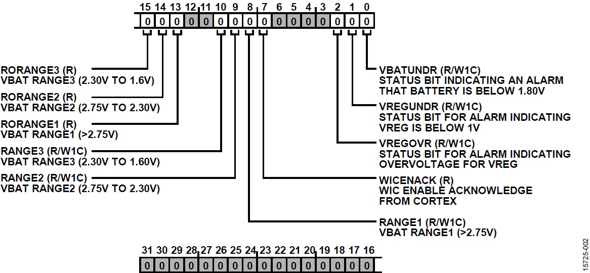
If the battery voltage is above 2.75 V, select 2.5 V as the reference. If the battery voltage is less than 2.75 V, select 1.25 V as the reference.
Fast Discharge of the Internal Reference Buffer
The ADuCM3027/ADuCM3029 MCU allows fast switching from a higher to a lower reference voltage. This switching is performed by enabling the fast discharge bit in the ADC configuration register (set Register ADC_CFG, Bit FAST_DISCH to 1).
The fast discharge can be enabled when switching:
- From 2.5 V to 1.25 V.
- From VBAT to 1.25 V.
- From VBAT to 2.5 V (if VBAT > 2.5 V).
For example, when switching from 2.5 V to 1.25 V at room temperature, the switchover time reduces by 2% (from 45 ms to 0.9 ms).
External Reference Voltage
To select an external reference voltage, disable the internal reference buffer by setting the internal reference enable bit in the ADC configuration register (Register ADC_CFG, Bit REFBUFEN) to zero. The external reference must not be more than the battery voltage. The external reference source must be connected to the VREF_ADC pin and it must be floating when the internal buffer is being used. Disabling the internal reference buffer reduces the power consumption of the ADC subsystem by approximately 200 μA.
PCB Recommendation
It is recommended to decouple the VREF_ADC pin with a 4.7 μF capacitor in parallel with a 0.1 μF capacitor very close to the GND_VREFADC pin, which in turn must be tied to the other GND pins (GND_DIG, GND_ANA, and the exposed pad) on the ADuCM3027/ADuCM3029. To achieve the best performance from these decoupling components, they must be placed as close as possible to the device, ideally right up against the device.
Selection of the Sampling Clock
The quality of the sampling clock in terms of jitter determines the ADC performance. Optimal selection of the sampling clock is critical based on the choice of application. Jitter is the variation of the placement of the clock edges, which results in a sampling time error. This uncertainty in the sampling edges leads to non-uniformly spaced samples and degrades the converter noise performance.
The clock jitter can be estimated by observing the degradation in the noise performance of the converter. SNR limitations due to jitter can be determined by the following equation:

where:
fIN is the input frequency.
tJITTER(RMS) is the rms jitter of the sampling clock.
For an ideal 12-bit ADC with a sampling rate of 154 kSPS, the clock jitter requirement is approximately 412 ps for an input frequency of 70 kHz, whereas if the input frequency is 300 Hz, the jitter requirement is approximately 105 ns.
A traditional way of observing clock jitter is by looking at it spectrally, as shown in Figure 3. In this diagram, because of the jitter present in the sampling clock, the ideal impulse response is spread out, resulting in spectral leakage. Much of the energy is distributed close to the desired frequency (this is known as close in noise) and much is also contained in the wide bandwidth broadband (known as wideband noise). The close in phase noise smears the fundamental signal into a number of frequency bins, which reduces the overall spectral resolution.


The sampling process is a multiplication of the sampling clock and the analog input signal. This multiplication in the time domain is equivalent to convolution in the frequency domain. Therefore, when the spectrum of the sampling clock is convolved with a pure sinewave input signal spectrum, the resultant spectrum also contains the spectral leakage of the sampling clock spectrum. Due to this leakage, the noise performance of the converter is degraded.
Figure 4 and Figure 5 show the effects of clock jitter on the spectrum of ADC samples. The ADC is enabled in oversampling mode to obtain 16-bit samples, and an input signal of 157 Hz is sampled at 604 SPS. When a free running oscillator with a jitter of approximately 4 ns over a period of 1 sec is used to sample the input frequency, the SNR of the sampled signal is degraded, as shown in Figure 4. In the same setup, if a clock source with considerably less jitter (approximately 200 ps) is used to sample the input signal, the degradation seen in the spectrum for the previous case is not observed (as shown in Figure 5).


Refer to the AN-756 Application Note, Sampled Systems and the Effects of Clock Phase Noise and Jitter, for more information.
Power Optimization
Another factor that can optimize the performance of the ADC in an ultra low power MCU is the power consumption. The following sections describe the various features present in the ADuCM3027/ADuCM3029 microcontrollers to reduce the overall power consumption of the system.
Low Power Mode in the Reference Buffer
The reference buffer offers a capability whereby the buffer consumes less current when compared to the regular mode of operation. This low power mode of operation can be enabled by setting the RBUFLP bit field of the reference buffer low power mode register (Register ADC_CFG1) to 1.
Flexi Mode
When the ADC is converting multiple samples, the DMA can be enabled to transfer the samples from the ADC output buffer to the memory. During this time, the ARM Cortex-M3 core can be put into Flexi mode or can be used for any other functions, reducing the overall power consumption. In Flexi mode, the core is sleeping and the rest of the peripherals and the DMA are still clocked. Therefore, DMA transfers can continue between peripheral and memory as well as from one memory location to another memory location.
High Power Buck
The high power buck (HP buck) is a capacitive buck converter, which reduces the overall current consumption of the device based on the VBAT level. For battery voltages above 2.8 V, the current consumption of the device decreases by approximately 50%.
Implementation of the Oversampling and Averaging Technique
Programming Flow for Oversampling
The following steps describe how to perform averaging over multiple conversions on a single channel.
- Set the ADC clock divider in the clock control register (Register CLKG_CLK_CTL1, Bit ACLKDIVCNT) to define the ADC clock ACLK, as given in the following equation:

where Root Clock is the root clock frequency (26 MHz), and can be sourced from HFOSC, HFXTAL, PLL or an external general-purpose input/output (GPIO) clock source. By default, the root clock is HFOSC.


Figure 6. CLKG_CLK_CTL1 Register. The sampling rate of the ADC is internally calculated from ACLK, in which the acquisition phase is Register ADC_ CNV_TIME, Bit SAMPTIME + 1 ACLK cycle, and the conversion phase is 13 ACLK cycles taken by successive approximation. The conversion phase is initiated at the end of the acquisition phase. The sampling rate is calculated by the following equation:

The oversampling factor determines the number of samples to be oversampled and averaged. It can take values from 1 to 256.
If the delay time is given in between ADC samples, the sampling rate must be calculated by the following equation:

Note that the Delay Time cannot take a value less than 1.
- Set the power-up ADC bit in the ADC configuration register (Register ADC_CFG, Bit PWRUP) to 1 to power up the ADC (see Figure 7).

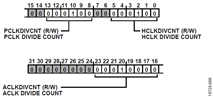
Figure 7. ADC Configuration Register Diagram. - Set the wait bits of the ADC power-up time register (Register ADC_PWRUP, Bits WAIT) as 526 divided by Register CLKG_CLK_CTL1, Bit PCLKDIVCNT.

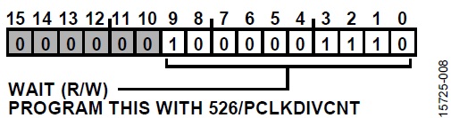
Figure 8. ADC_PWRUP Register. Power-up wait is necessary for proper functioning of the ADC. If Register CLKG_CLK_CTL1, Bit PCLKDIVCNT is 1, the maximum power-up wait time needed for the ADC is 526 clock cycles.
- Select the internal 1.25 V or 2.5 V reference buffer as the reference voltage using the VREFSEL bit in Register ADC_ CFG.
- Enable the internal reference buffer by setting the REFBUFEN bit in Register ADC_CFG.
- Enable low power mode for the reference buffer by setting
the RBUFLP bit in Register ADC_CFG1.

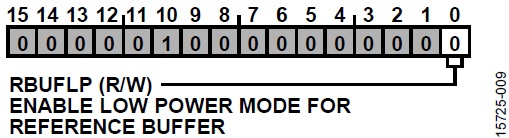
Figure 9. ADC_CFG1 Register Diagram. - Enable the ADC subsystem by setting the EN bit in Register ADC_CFG.
- Wait 3.5 ms. The wait time is required by the internal reference buffer to reach the set reference buffer voltage level (1.25 V or 2.5 V). One of the general-purpose (GP) timers can be used to wait for 3.5 ms. During this wait period, the device can be put into Flexi mode to save system power, and can be woken up by the GP timer interrupt.
- Check the state of the ADC ready to start converting bit on the ADC status register (Bit RDY, Register ADC_STAT). If it is 1, the ADC is ready to start converting.
- Write 1 to clear the RDY bit on Register ADC_STAT (see
Figure 10).

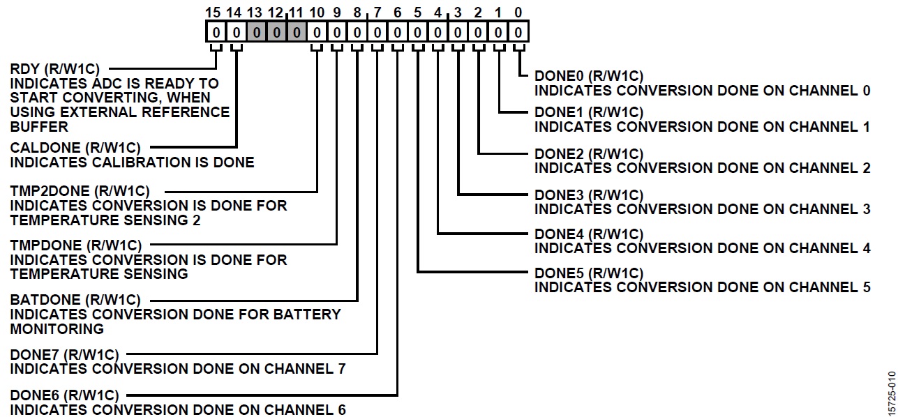
Figure 10. ADC_STAT Register Diagram. - Set the STARTCAL bit on Register ADC_CFG to start the calibration cycle.
- Check the CALDONE bit on Register ADC_STAT. If it is asserted, write 1 to clear the bit.
- Set the SEL bits in the ADC conversion configuration
register, Register ADC_CNV_CFG (shown in Figure 11), to select a channel for conversion. For example, writing 1
to these bits selects Channel 0.

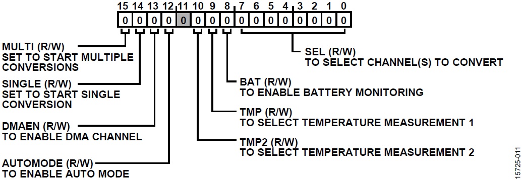
Figure 11. ADC_CVN_CFG Register Diagram. - Set the CNVDONE bit to 1 in the ADC interrupt enable register (Register ADC_IRQ_EN) to enable the interrupt function when the conversion is complete (see Figure 12).


Figure 12. ADC_IRQ_EN Register Diagram. - Set the OS and EN bits to 1 in the ADC averaging configuration register (ADC_AVG_CFG) to enable oversampling and averaging (see Figure 13).

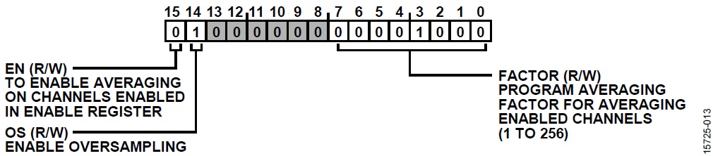
Figure 13. ADC_AVG_CFG Register Diagram. - Set the oversampling and averaging factor (M) in the FACTOR bit fields in the ADC averaging configuration register (ADC_AVG_CFG). The factor to be programmed for a required resolution is given in Table 1.
Table 1. Oversampling and Averaging Factor for Enhanced Resolution Resolution Required Oversampling and Averaging Factor (M) Number of Samples Used for Averaging 13-Bit 0x02 4 14-Bit 0x08 16 15-Bit 0x20 64 16-Bit 0x80 256 - Set the SINGLE bit in Register ADC_CNV_CFG to 1 to start a single conversion.
- The conversion done interrupt is generated if the CNVDONE bit in the ADC_IRQ_EN register is set. Check the conversion done bit in the ADC_STAT register for the corresponding channel (for example, Register ADC_STAT, Bit DONE0) when the conversion done interrupt is generated.
- Read the conversion output from the conversion result register of the corresponding channel (for example, ADC_CH0_OUT).
- Write 1 to clear the conversion done bit in the ADC_STATregister (for example, set Bit DONE0 to 1).
- To obtain multiple oversampled and averaged samples, repeat Step 1 to Step 15.
- Set the following DMA configurations:
- DMA count = 9 for ten conversions (DMA count = number of conversions − 1).
- Source address = address of ADC_DMA_OUTregister.
- Source size = half word.
- Set the destination address of DMA as the SRAMmemory location address to store the conversion result.
- Program the required increment in the destination address.
- Set the DMAEN bit in Register ADC_CNV_CFG to 1 in the ADC conversion configuration register and enable the DMA.
- Set the MULTI bit in Register ADC_CNV_CFG to 1 in the ADC conversion configuration register to start the conversion.
- When DMA_DONE interrupt is generated, clear the MULTI bit to disable further conversions in the interrupt service routine.


Application Example Overview
This section describes an application sequence to perform ADC oversampling and averaging in power optimized mode.
In this example, ADC is enabled in oversampling and averaging mode. The oversampling factor (M) is set at 256 to obtain 16-bit samples. The DMA is configured to capture and store 1024 16-bit samples in SRAM locations. The samples are later obtained by means of the universal asynchronous receiver/transmitter (UART) interface. During ADC conversion and DMA transfers, the core is in Flexi mode.
The application flow for oversampling in multiconversion mode is shown in Figure 14.

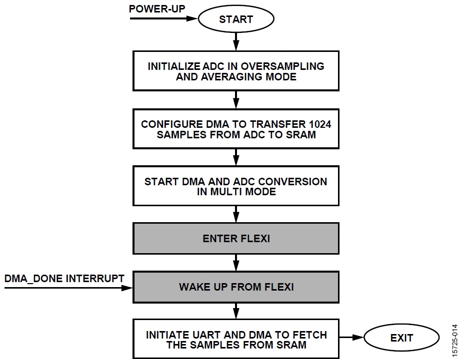
Figure 15 shows the application sequence.


Results
The ADC performance measurement describing ENOB vs. the oversampling and averaging factor is shown in Figure 16. The ENOB is calculated based on the signal-to-noise-and-distortion ration (SINAD), as described in Equation 1. The SINAD is obtained by inputting a sinewave signal with a frequency of 157 Hz from a signal generator to ADC Channel 0.

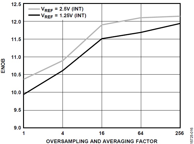
For each oversampling factor (M), the ADC clock frequency is adjusted such that the throughput is always 604 SPS.
Because the ADC is not ideal, to calculate the true ADC performance measure, SINAD is considered.
参考电路
Kester, Walt. The Data Conversion Handbook. Analog Devices, 2005.