AN-1456: Digital Dither Generation in the AD5766/AD5767
Introduction
The AD5766/AD5767 is a 16-channel, 12-bit/16-bit, denseDAC® digital-to-analog converter (DAC) that can be configured to generate multiple output voltage spans from a minimum voltage of −20 V to a maximum voltage of +14 V from an external +2.5 V reference, while delivering up to 20 mA of output current per channel.
The AD5766/AD5767 integrates an analog dither functionality to find the optimum dc bias point and keep the modulator in quadrature for indium phosphide Mach Zehnder modulators (InP MZMs), as described in the AN-1446 Application Note, Dither Generation in the AD576.
When the analog input frequency or amplitude specification of the analog dither input does not fulfill the application requirements for a given modulator range, a digital dither, or arbitrary waveform, can be generated by the DAC itself.
The purpose of this application note is to discuss the digital dither, in terms of generating an output signal.
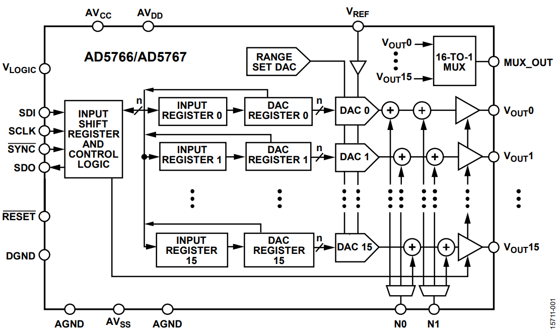
Figure 1 shows the block diagram of the AD5766/AD5767.

Dither Specifics in the AD5766/AD5767
How to Generate a Digital Dither
A sine, square, triangle, or arbitrary waveform can be generated digitally by continuously updating the DAC register. To guarantee a higher performance on the recomposed signal from the discrete samples generated using the DAC, some basic principles must be understood. The maximum update rate, or updates per second (UPS), must be limited to the settling capabilities of the output for a given resolution.
The first step is to analyze the steps involved in updating the VOUTx pins.
- A new value is written into the input register, as shown in Figure 2.

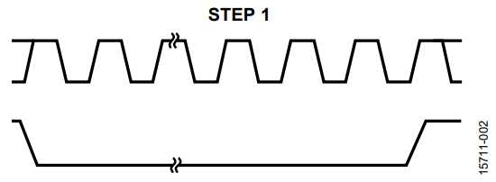
Figure 2. VOUTx Update, Step 1. - The digital block processes the command and updates the DAC register, as shown in Figure 3.

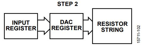
Figure 3. VOUTx Update, Step 2. - VOUTx voltage starts to settle to the voltage defined by the new code written in the register (see Figure 4).

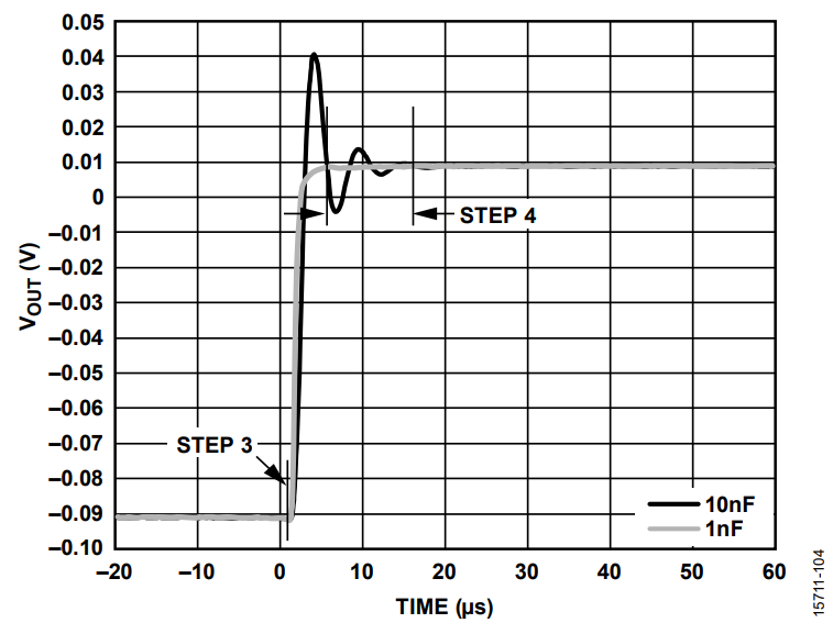
Figure 4. VOUTx Update, Step 3 and Step 4. - After a variable period of time (shown in Figure 4), the output becomes settled to the voltage defined by the new code within a tolerance range, typically ±0.5 LSB around the final code.


Generally, the shorter the time that causes the DAC to move from Step 1 to Step 4, the more samples, or updates per second, can be generated, which has two implications: first, the generated output signal becomes smoother as more outputs are generated; and second, a higher frequency can be generated.
How to Maximize the Update Rate
By default, the maximum updates per second that can be generated is limited by the time that it takes for the new code to move through all the steps in the previous section. This section provides an analysis of all the steps, and their impact on settling time.
Step 1 depends on the digital clock, and at the maximum clock rate (50 MHz), it can be as short as 20 ns × 24 bits = 480 ns, without considering other time restrictions, such as minimum SYNC high time. In this case, the maximum update rate is limited to 5 µs.
The output voltage settling time, as described in Step 2, Step 3, and Step 4, is included in the Specifications section of the AD5766/AD5767 data sheet for specific conditions. In this case, a code transition from ¼ to ¾ scale, the output voltage settling time is approximately 10 µs at a 0.5 LSB tolerance range.
In summary, the overall update time without any compression scheme can be considered approximately 10 µs for a 0.5 LSB error range.
The preceding update time can be improved, applying some compression techniques that can be used to optimize and minimize the update time.
The first technique is based on parallelizing activities; in this case, transferring a new code (Step 1) while the VOUTx voltage is still settling (Step 4).
This technique is known as lossless precision.
Based on the specifications in the AD5767 data sheet, the settling time conditions (Step 2, Step 3, and Step 4) refer to a 5 V step transition. When the DAC slew rate is 1 V/µs, the DAC takes approximately 5 µs to process the command (Step 2), and approximately another 5 µs for the VOUTx to become settled (Step 3 and Step 4).
Note that the 5 µs settling time is for a ½ scale transition. The time it takes for another voltage transition can be calculated as follows:
1 µs × ΔVOUTx = settle time
In this case, the update rate timing is 10 µs − 480 ns = 9.52 µs for a 5 V setup.
Figure 5 shows the principle of this lossless precision technique, which is recommended for small step changes, typical in sine, sawtooth, or triangular signal generations.

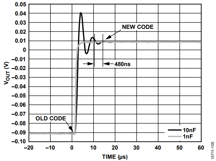
The other compression technique is more aggressive, and results in a penalty to the effective DAC resolution. This method is based on updating the DAC just before the previous command is processed. In this case, the update rate can be as high as 5 µs – 480 ns, which is the digital process command time, as shown in Figure 6. This approach is recommended for large step transitions, such as square wave generation.

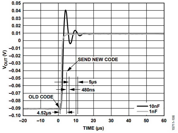
However, this technique has three drawbacks: the output is not fully settled; the gain bandwidth (GBW) of the amplifier must be considered; and digital-to-analog glitches and digital feedthrough effects are not negligible.
Practical Example
To generate a digital signal, several factors must be considered, such as output frequency, update rate, and number of channels.
To generate a 1 kHz sine wave signal in a single channel, assuming 10 samples per period, the update rate is 10,000 UPS. The output signal is shown in Figure 7.

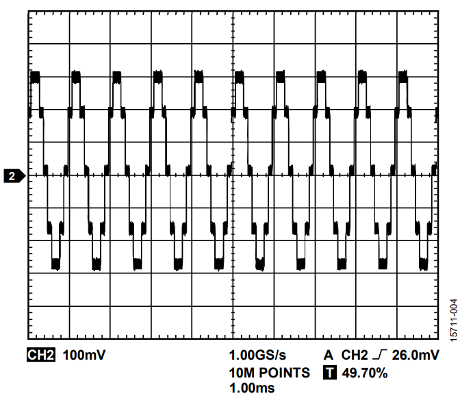
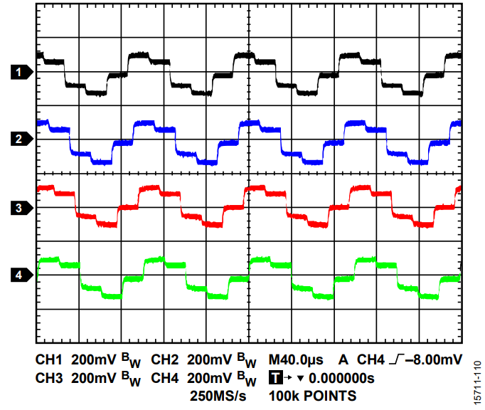
To generate a 20 kHz sine wave signal, assuming 9 samples per period, the update rate is 180,000 UPS. The output signal is shown in Figure 8.

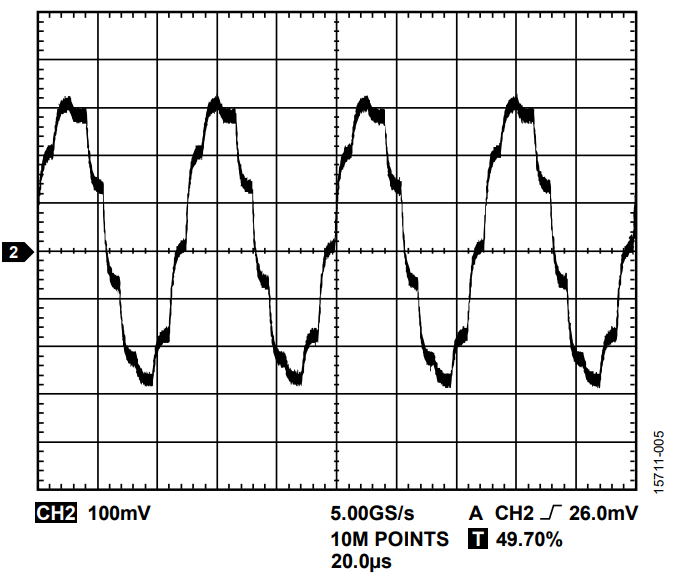
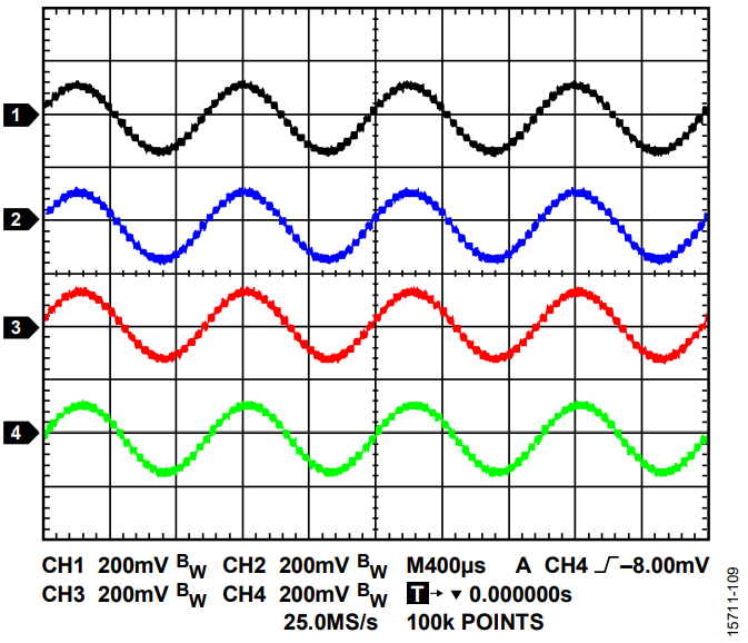
To generate a 10 kHz sine wave signal, assuming 7 samples per period and 4 channels, the update rate is 1 × 25 × 4 = 100,000 UPS. The output signal is shown in Figure 9.

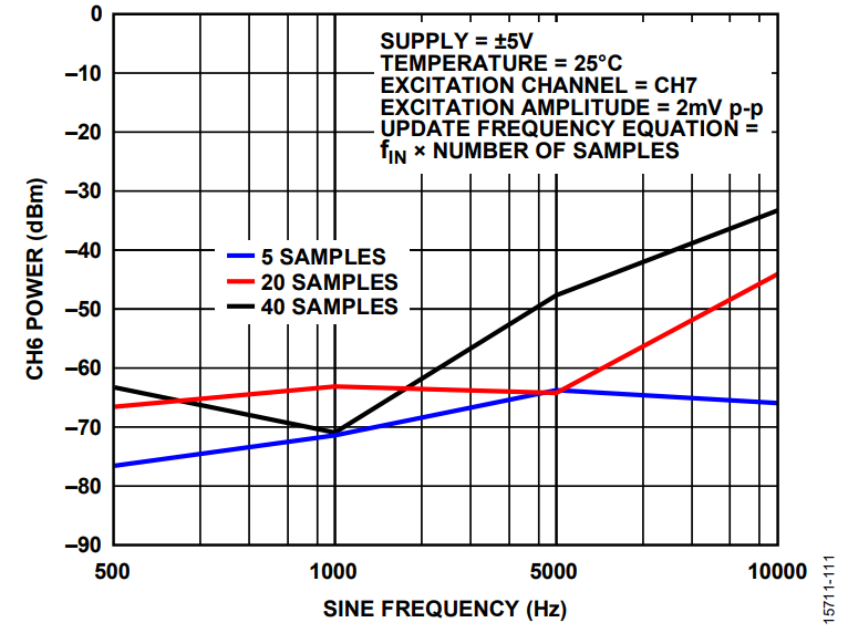
To compare the performance in terms of frequency and samples per period (in this case, five),see Figure 10.

Note that the phases for the different channels in Figure 9 and Figure 10 have not been matched; therefore, all the sine waves are generated with Phase 0. As the channels are updated sequentially, a phase delay is observable.
DAC Outputs Effects
When the digital signal is generated, the crosstalk generated can be observed in adjacent channels, especially at the update rate frequency, which is typically the higher tone, as shown in Figure 11.

作者
