AN-1453: Programming the ADM1266 Firmware and Configuration via the PMBus
Introduction
This application note details the steps required to program firmware and configuration on the ADM1266 in a mass programming environment or in a system application. The firmware and configuration updates can be performed individually based on the requirement.
Hardware Setup
Figure 1 shows the recommended pin settings for the ADM1266 for a mass programming environment, only. It is recommended that all components used in the hardware setup are surface-mount components.

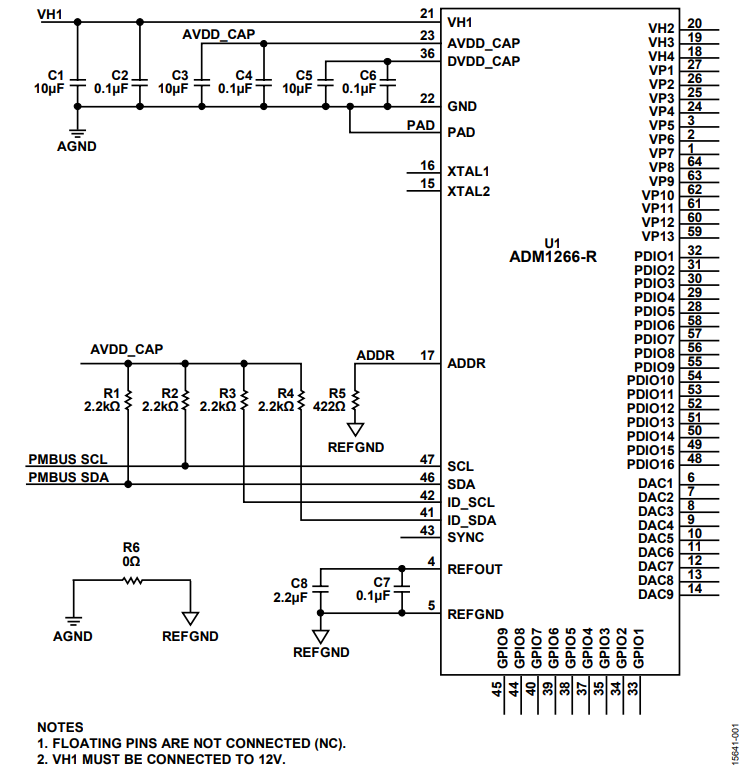
The PMBus address of the ADM1266 is set by connecting an external resistor (R5) from the ADDR pin to GND. Table 1 lists the recommended resistor values and associated PMBus addresses.
| PMBus Address | 1% Resistor (kΩ), E96 Series |
| 0x40 | 0.422 |
| 0x41 | 1.5 |
| 0x42 | 2.67 |
| 0x43 | 4.12 |
| 0x44 | 5.36 |
| 0x45 | 7.15 |
| 0x46 | 8.87 |
| 0x47 | 10.7 |
| 0x48 | 12.7 |
| 0x49 | 14.7 |
| 0x4A | 16.9 |
| 0x4B | 19.1 |
| 0x4C | 21.5 |
| 0x4D | 24.3 |
| 0x4E | 27.4 |
| 0x4F | 31.6 |
Memory Partition
Figure 2 shows an overview of the memory partition applicable to this application note.

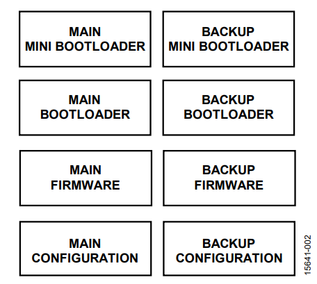
The ADM1266 is preprogrammed with the mini bootloader and bootloader only. The mini bootloader and bootloader are not upgradable by the user.
When the ADM1266 is preprogrammed with only bootloaders, the ADM1266 must first be programmed with firmware, followed by the configuration data.
The firmware and configuration for the ADM1266 is generated by ADI Power Studio® graphical user interface (GUI) software, which is available for download from the EVAL-ADM1266 evaluation board product page.
The same firmware is used for all devices, and a different configuration is used for different devices.
Reading the .hex File
The .hex files generated for the firmware and the configuration follow the Intel® hexadecimal format.
Each line of the .hex file contains a hexadecimal number that encodes multiple binary numbers for representing the data and the register address where the data must be written.

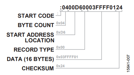
The end of the .hex file is represented by :00000001FF. The PMBus write type is based on the byte count, such as 1 byte results in a byte write, 2 bytes result in a word write, and 3 or more bytes result in a block write.
Programming Firmware
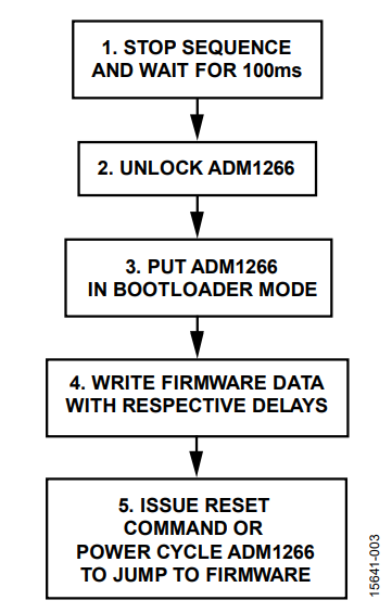
The ADM1266 is powered up in bootloader mode and stays in bootloader mode if no firmware is present. As shown in Figure 4, only Step 4 and Step 5 are required to load the firmware.

Step 1: Stop the Sequence Before Firmware Upgraded
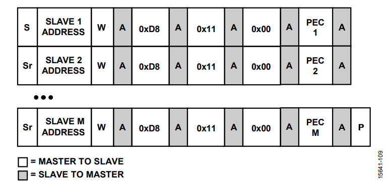
Before the firmware is updated via the PMBus, the current sequence must be stopped. The sequence is stopped by writing 0x0003 to the GO_COMMAND command (Register 0xD8). A group command can be issued to stop multiple ADM1266 devices on the same PMBus simultaneously, as shown in Figure 5.

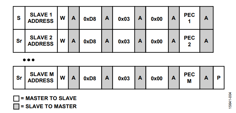
If the group command cannot be issued, each ADM1266 device can be stopped individually.
After issuing a stop command, it is required to wait for 100 ms before sending the next PMBus command.
Step 2: Unlock the ADM1266
The ADM1266 must be unlocked before the firmware can be updated.
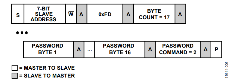
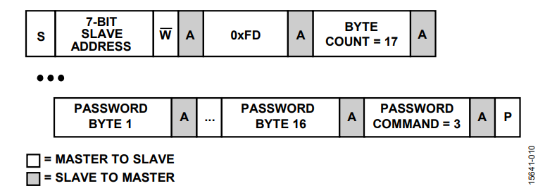
The ADM1266 can be unlocked by performing two consecutive writes of the correct password to the FW_PASSWORD command (Register 0xFD). The block write command to unlock the ADM1266 is shown in Figure 6. The default password is 0xFF for the first 16 bytes, and the 17th byte (password command) is set to 0x02.

The unlock status can be confirmed by the PART_LOCKED bit (Bit 2) of the STATUS_MFR_SPECIFIC command (Register 0x80), which is set to 0 when the ADM1266 is unlocked. See Table 5 for more information.
Step 3: Place the ADM1266 in Bootloader Mode
The ADM1266 must be placed in bootloader mode before the firmware can be programmed. The ADM1266 can be placed in bootloader mode by writing 0x02, 0x00, and 0x00 to the UPDATE_ FW command (Register 0xFC) as a group command, as shown in Figure 7.

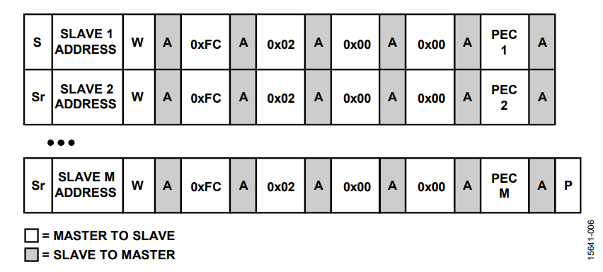
If the command cannot be issued, each ADM1266 device can be placed in bootloader mode individually.
Step 4: Delays Between Writing Firmware Data
When the firmware is programmed in the ADM1266 via the PMBus, the user is not required to erase the EEPROM. The bootloader automatically erases the EEPROM pages that are reserved for firmware when the bootloader receives the first stream of firmware data. Table 2 states the respective delays between writing data.
| Command | Wait Time Required Before Writing Next Block of Data |
| First Write to 0xFC (UPDATE_FW) | 2 sec |
| Subsequent Writes to 0xFC | 40 ms |
Step 5: Issue a Reset Command or Power Cycle After Programming Firmware
After the firmware data is successfully written to the ADM1266, it is required to issue a reset command or power cycle before programming the configuration data.
The ADM1266 can be reset by writing 0x0004 to the GO_COMMAND command (Register 0xD8).
Programming the Configuration
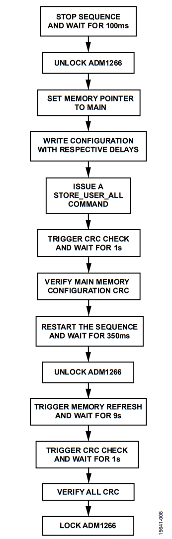
See Figure 8 for the flowchart for programming the configuration.

Follow the procedures detailed in the Step 2: Unlock the ADM1266 section and the Reading the .Hex File section.
Stop the Sequence Before Programming the Configuration Data
Before the configuration is programmed via the PMBus, the current sequence must be stopped. There are two options for stopping the sequence: seamless update reset stop and soft reset stop. When updating the configuration, it is recommended to use seamless update reset stop, which causes the sequence to jump directly to the power-good state of the new configuration when the sequence is resumed.
In a seamless update reset stop, the sequence is stopped by writing 0x0011 to the GO_COMMAND command (Register 0xD8) as a group command to stop multiple ADM1266 devices on the same PMBus simultaneously, as shown in Figure 9.

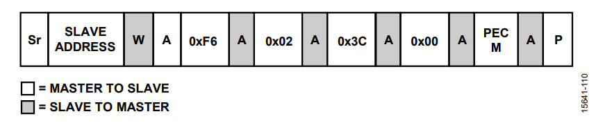
Seamless update reset stops have a default timeout of 10 minutes. If the sequence is not resumed by the user, the sequence automatically resumes after the timeout expires. The timeout value can be updated using the HITLESS_TIMEOUT command (Register 0xF6) before stopping the sequence.
Figure 10 shows an example for setting the reset time to 60 sec.

It is only recommended to use a soft reset stop in a mass programming environment or when there is no previous configuration programmed.
In a soft reset stop, the sequence is stopped by writing 0x0003 to the GO_COMMAND command (Register 0xD8) as a group command to stop multiple ADM1266 devices on the same PMBus simultaneously, as shown in Figure 9.
If the group command cannot be issued, each ADM1266 device can be stopped individually.
After issuing a stop command, it is required to wait for 100 ms before sending the next PMBus command.
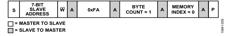
Setting the Memory Pointer to Main Memory
The configuration data for the ADM1266 must be programmed to the main memory. If the configuration data in the main memory is valid, the ADM1266 always runs the configuration from the main memory. If the configuration data in the main memory is corrupt and the configuration data in the backup memory is valid, the ADM1266 runs the configuration data from the backup memory.
The memory pointer can be set to the main memory by using the SWITCH_MEMORY command (Register 0xFA), as shown in Figure 11.

Delays Between Writing Data
When the configuration data is programmed in the ADM1266 via the PMBus, the user is not required to erase the EEPROM.
The firmware automatically erases the EEPROM pages based on the data sent to the ADM1266. The typical time needed to erase one EEPROM page is 50 ms.
Due to the time needed for the automatic erase of the EEPROM, the user is required to wait for a specific time before sending the next stream of data.
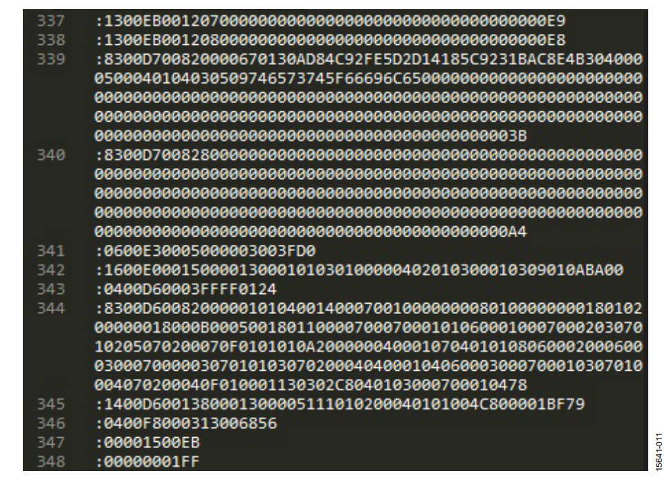
Table 3 states the typical delay that must be maintained after writing to specific commands and the corresponding line number in the sample .hex file shown in Figure 12.
| Command | Wait Time Required Before Writing Next Block of Data | Line Number in .hex File (See Figure 12) |
| 0xD7 (SYSTEM_CONFIGURATION) | 400 ms (after first write) | 339 |
| 0xE3 (USER_DATA) | 100 ms (after first write) | 341 |
| 0xE0 (LOGIC_CONFIGURATION) | 200 ms (after first write) | 342 |
| 0xD6 (SEQUENCE_CONFIGURATION) | 2.5 sec (after first write) | 343 |
| 0xF8 (MEMORY_CONFIG) | 100 ms | 346 |
| Subsequent Writes to 0xD7, 0xE3, 0xE0, 0xD6 | 40 ms | 340, 344, 345 |
| 0x15 (STORE_USER_ALL) | 300 ms | 347 |

After the configuration write is complete, issue a send command to the STORE_USER_ALL command (Register 0x15) to commit the system configuration settings to the EEPROM.
Verifying the Updated Main Memory Configuration Data
Verification is required only when updating the configuration. Verification of the updated main memory configuration data is optional when no previous configuration is programmed in the ADM1266.
After writing the configuration data, cyclic redundancy check (CRC) calculations of all the memory sections can be triggered by writing to the MEMORY_RECALCULATE_CRC command (Register 0xF9), as shown in Figure 14.
Allow 1 sec to elapse before reading the status of the memory CRC, which can be check by a word read of the STATUS_MFR_ SPECIFIC_2 command (Register 0xED). Bit mapping for this register is detailed in Table 4. Verify that the MAIN_PROJECT_ CRC_FAULT bit and the MAIN_ABCONFIG_CRC_FAULT bit are set to 0. These bits being set to 0 indicates that the main memory configuration was written successfully.
| Bit | Bit Name |
| 15 | BKUP_PASSWORD_CRC_FAULT |
| 14 | BKUP_FIRMWARE_CRC_FAULT |
| 13 | BKUP_PROJECT_CRC_FAULT |
| 12 | BKUP_ABCONFIG_CRC_FAULT |
| 11 | MAIN_PASSWORD_CRC_FAULT |
| 10 | MAIN_FIRMWARE_CRC_FAULT |
| 9 | MAIN_PROJECT_CRC_FAULT |
| 8 | MAIN_ABCONFIG_CRC_FAULT |
| 7 | BKUP_IAP_CRC_FAULT |
| 6 | BKUP_MINI_IAP_CRC_FAULT |
| 5 | MAIN_IAP_CRC_FAULT |
| 4 | MAIN_MINI_IAP_CRC_FAULT |
Restarting the Sequence After Updating
When the new configuration data is written to the ADM1266, the new sequence can be run by writing 0x0000 to the GO_ COMMAND command (Register 0xD8) as a group command to restart the sequence in multiple ADM1266 devices simultaneously. The group command protocol is shown in Figure 5.
If the group command cannot be issued, each ADM1266 device can be restarted individually.
If the sequence is stopped using seamless update reset stop, the sequence jumps directly to the power-good state defined in the configuration when restarted. If the no power-good state is defined, the sequence starts from the first user state.
If the sequence is stopped using soft reset stop, the sequence starts from the first user state when restarted, causing the board to power cycle.
After restarting the sequence, wait 350 ms before sending the next PMBus command.
Triggering Memory Refresh
The ADM1266 contains backup memory sections for the mini bootloader, bootloader, firmware, and configuration. After the firmware and configuration are successfully programmed, trigger memory refresh. Memory refresh copies the main memory content to the backup memory, and the backup memory to the main memory.
Confirm that the ADM1266 is unlocked before triggering the memory refresh. See the Step 2: Unlock the ADM1266 section.
Memory refresh for all the memory sections can be triggered by performing a block write to the REFRESH_FLASH command (Register 0xF5), as shown in Figure 13.

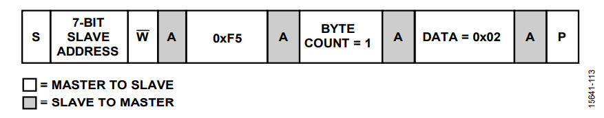
A memory refresh requires approximately 9 sec to complete. Check the status of the memory refresh by reading the RUNNING_REFRESH bit in the STATUS_MFR_SPECIFIC command (Register 0x80). If the RUNNING_REFRESH bit is set to 1, memory refresh is still running. Wait until this bit is set to 0 before proceeding.
Verifying Firmware and Configuration Data
After writing the firmware, configuration data, and triggering a memory refresh, CRC calculations of all the memory sections can be triggered by writing to the MEMORY_RECALCULATE_CRC command (Register 0xF9), as shown in Figure 14.

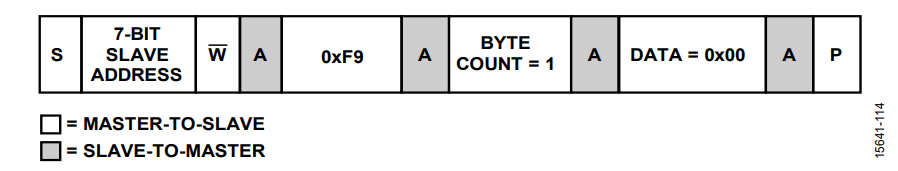
Allow 1 sec to elapse before reading the status of the memory CRC. To check the status of the memory CRC, perform a word read of the STATUS_MFR_SPECIFIC_2 command (Register 0xED). The bit mapping for this register is detailed in Table 4.
ALL_CRC_FAULT is a single bit that is an OR of all the CRC bits shown in Table 4. This bit can read from the STATUS_ MFR_SPECIFIC command (Register 0x80).
Check the status of the configuration compatibility (Bit 1) and silicon compatibly (Bit 0) by reading back the STATUS_MFR_ SPECIFIC command (Register 0x80).
| Bit | Bit Name |
| 5 | ALL_CRC_FAULT |
| 4 | TESTMODE_ENABLED |
| 3 | RUNNING_REFRESH |
| 2 | PART_LOCKED |
| 1 | PART_DATA_COMPATIBLE_FAULT |
| 0 | SILICON_COMPATIBLE_FAULT |
If the CRC and compatibility pass, the bit in which they passed is set to 0. If the CRC and compatibility fail, the bit in which they failed is set to 1.
The firmware version number can be read back from the IC_ DEVICE_REV command (Register 0xAE). Use a block read to validate that the firmware is updated to the correct revision. The byte mapping for the command is shown in Table 6.
| Byte Name | Byte | Example | Notes |
| Data Length | Byte 0 | 0x08 | Fixed to 0x08 |
| Firmware Revision | Byte 1 | 0x01 | Indicates Version 1.8.7 |
| Byte 2 | 0x08 | ||
| Byte 3 | 0x07 | ||
| Bootloader Revision | Byte 4 | 0x00 | Indicates Version 0.0.7 |
| Byte 5 | 0x00 | ||
| Byte 6 | 0x07 | ||
| Chip Revision | Byte 7 | 0x42 | Indicates Version B0 |
| Byte 8 | 0x30 |
Locking the ADM1266
After a power cycle, the ADM1266 is automatically locked. The ADM1266 can also be locked by writing any 16 bytes of data, and the 17th byte (password command), which is set to 0x03, once to the FW_PASSWORD command (Register 0xFD). The block write command for locking the ADM1266 is shown in Figure 15.

The lock status can be confirmed by the PART_LOCKED bit (Bit 2) of the STATUS_MFR_SPECIFIC command (Register 0x80), which is set to 1 when the device is successfully locked.
Packet Error Checking (Pec) Control (Optional)
If the user has the capability to recognize acknowledge bits and no acknowledge bits in the I2C communication, it is recommended to use the PEC byte for all writes to ensure proper data transfer.
The PMBus controller implements PEC to improve reliability and communication robustness. The PEC is implemented by appending a PEC byte at the end of the message transfer. The PEC byte is calculated using a CRC-8 algorithm on all address, command, and data bytes from the start bit to the stop bit.
This process excludes the acknowledge, no acknowledge, start, restart, and stop bits. The PEC byte is appended to the end of the message by the device that supplied the last data byte. The receiver of the PEC byte is responsible for calculating the internal packet error code and comparing this code to the received PEC byte.
The PMBus slave device can communicate with master PMBus devices that support PEC, as well as those that do not support PEC. If a PEC byte is available, the PMBus checks the PEC byte and acknowledges if it is correct. If the PEC byte comparison fails, the PMBus device does not acknowledge the PEC byte and does not process the command sent from the master.
The PMBus uses built in hardware to calculate the PEC code using the CRC-8 polynomial, C(x) = x8 + x2 + x1 + 1. The PEC code is calculated one bye at a time, in the order that it is received. In a read transaction, the PMBus appends the PEC byte following the last data byte. In a write transaction, the PMBus compares the received PEC byte to the internally calculated PEC code.
作者

