AN-1443: Interfacing an SD Card Through the ADuCM3027/ADuCM3029 SPI Bus
Introduction
Secure digital (SD) cards are the most common flash-based storage devices used in portable devices and embedded systems. An SD card is an ideal solution for storage requirements due to its small size, low power, simplicity, and low cost. The compatibility of the SD card with most devices makes it easier to access and retrieve data from the card using any computer for further processing according to the application.
This application note discusses how to use the serial peripheral interface (SPI) of the ADuCM3027/ADuCM3029 processor to interface with SD cards.
This application note details general information about SD cards such as pinouts, communication standards, and design considerations, and it also discusses SPI basics, such as signals and waveforms, and the features of the ADuCM3027/ ADuCM3029 SPI interface.
Required Boards

SD Cards
The SD card is a memory card that was introduced in 1999 by the SD Association (SDA) to extend the capabilities of the multimedia card (MMC) for use in portable devices. Since then, the SD card has been widely accepted and it has become the industry standard that most portable devices now use an SD card to store files such as pictures, music files, and so on.
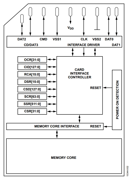
SD cards are composed of a pin interface, memory core, internal registers, and an internal controller, as shown in Figure 2. The memory core is the storage for data and comes in different sizes, from 1 MB to 2 TB. The internal registers store the SD card status. The pin interface is the connection between the card and the master device, normally a microcontroller, which uses the card.
The card interface controller manages the core memory of the SD card. This controller usually handles the writing, reading, and erasing of data in the flash, error handling, and flash wear levering. Therefore, the main microcontroller that implements the SD card sends commands and data to the card interface controller through a sequence of data packets and does not care about the management of the memory core.

Capacity and Type
SD cards are available in different types, sizes and capacities. The types of the SD cards can depend on memory capacity and the SD standards they are complying to.
Table 1 describes different types of SD cards and their capacities.
| Common SD Card Type | Capacity |
| SD Standard Capacity (SDSC) | 1 MB to 2 GB |
| SD High Capacity (SDHC) | 2 GB to 32 GB |
| SD eXtended Capacity (SDXC) | ≥32 GB |
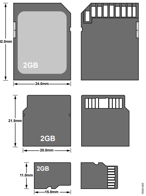
SD cards are also available in different form factors and sizes, such as the standard size, mini size, and the micro size, as shown in Figure 3.

Interfaces and Modes
SD cards have a pin interface that have different pinout configurations depending on what communication mode and card form factor is used. Typically, the interface is composed of power lines (supply and ground), a clock line, data lines, and command lines. On the newer high speed cards, a low voltage differential interface is implemented to cater to high speed and high bandwidth transfers.
Communication with SD cards is normally done in SD bus mode, which is an interface defined by the SDA. In this mode, the interface has a separate command and data line and clock line. Transfers have a proprietary format; however, it is difficult to implement this format on embedded systems with no native SD interface.
To support the embedded systems and microcontrollers that have no native SD interface, the SDA also defines in its specifications that SD cards must support SPI bus mode. In this mode, the SD card operates over the well known SPI widely used by microcontrollers. However, SPI bus mode supports only a subset of the full SD card standard protocols.
Figure 4 shows a pinout for the standard SD card pinout and a micro SD card pinout.

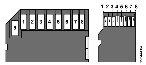
The pinout for the standard SD card is described in Table 2.
| Pin No. | Name | SD Mode | SPI Mode |
| 1 | CS/DAT3 | Data Line 3 | Chip select |
| 2 | CMD/DI | Command line | MOSI |
| 3 | VSS1 | Ground | Ground |
| 4 | VDD | Supply voltage | Supply voltage |
| 5 | CLK | Clock | Clock (SCK) |
| 6 | VSS2 | Ground | Ground |
| 7 | DAT0 | Data Line 0 | MISO |
| 8 | DAT1 | Data Line 1 | Unused or IRQ |
| 9 | DAT2 | Data Line 2 | Unused |
The pinout for the micro SD card is described in Table 3.
| Pin No. | Name | SD Mode | SPI Mode |
| 1 | DAT2 | Data Line 2 | Unused |
| 2 | DAT3/CS | Data Line 3 | Chip select |
| 3 | CMD | Command line | MOSI |
| 4 | VDD | Supply voltage | Supply voltage |
| 5 | CLK | Clock | Clock (SCK) |
| 6 | VSS | Ground | Ground |
| 7 | DAT0 | Data Line 0 | MISO |
| 8 | DAT1 | Data Line 1 | Unused or IRQ |
SD Card SPI Protocol
The SD protocol used in SPI bus mode is somewhat different from the protocol used in SD bus mode. Communication with the SD card in SPI bus mode is a simple command response protocol that is initiated by the master device (microcontroller) by sending a command frame. When the SD card receives the command frame, the card responds by sending a response frame or an error frame depending on the command that was sent by the host microcontroller.
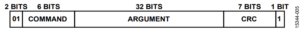
The SD card command frame is composed of a 6-byte structure that is sent to the SD card. The command frame always starts with Bits 01 followed by a 6-bit command number. The initial byte packet is followed by a 4-byte argument that is in big endian format. The last byte is composed of the 7-bit cyclic redundancy check (CRC) and a 1 stop bit address (see Figure 5).

The SD card responds to each command frame with a response frame that differs according to the command frame sent. In SPI bus mode, only three response types can be used: R1, R3, and R7 (see Figure 6).

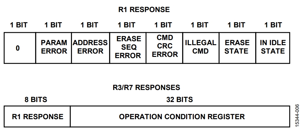
Next, the SD card sends the R1 response token after every command, with the exception of the SEND_STATUS command. This command is one byte long, and the most significant bit (MSB) is always set to 0. The other bits are error indications; an error is indicated by a 1. The meaning of the error flags are defined as follows:
- Idle state: the card is in the idle state and running the initializing process.
- Erase reset: an erase sequence was cleared before executing because an out-of-erase sequence command was received.
- Illegal command: an illegal command code was detected.
- Communication CRC error: the CRC of the last command failed.
- Erase sequence error: an error occurred in the sequence of erase commands.
- Address error: a misaligned address that did not match the block length was used in the command.
- Parameter error: the argument of the command (for example, address or block length) was outside of the allowed range for this card.
The SPI mode of the SD card uses only a subset of the commands used in SD mode. See Table 4 for the detailed list of commands for SPI mode. The command set is limited to initializing the card, retrieving some important details, and then reading or writing data blocks to the memory card.
| Command | Description |
| CMD0 | Reset card |
| CMD8 | Request for current operational conditions |
| CMD55 | Leading command for application specific commands (ACMDs) |
| ACMD41 | Start card initiation process |
| CMD58 | Request for operation conditions register (OCR) |
| CMD16 | Change block length |
| CMD17 | Read a block of data |
| CMD24 | Write a block of data |
| CMD32 | Set the start block to be deleted |
| CMD33 | Set the end block to be deleted |
| CMD38 | Start block erase set by CMD32 and CMD33 |
File Allocation Table (FAT) File System
Common available SD cards are formatted by default as FAT file systems. The FAT file system is a legacy file system that is widely supported by nearly all PCs, mobile devices, and embedded systems. A driver to support this file system can be small, robust, and lightweight, which can be easily implemented in a microcontroller or in an embedded system. Any saved files on the FAT formatted memory card are viewable and modifiable on virtually all PCs due to the support available for this basic file system.
The SD card specification defines the FAT file system type that can be used in different SD card by capacity (see the References section for additional information).
SDCard Implementation
ADuCM3027/ADuCM3029 SPI
The ADuCM3027/ADuCM3029 microcontroller has three SPI interfaces (SPI0, SPI1, and SPIH) that can be used to communicate with various SPI-compatible devices, such as high speed sensors and memory devices. Each SPI port has four hardware chip select signals that control the four SPI-compatible devices. The SPI bus peripherals also include programmable baud rates, clock phase, and clock polarity, different mechanisms of hardware flow control, and it can act as an SPI master or slave.
The three SPIs are identical from an SPI programming and model perspective, except for the internal bus interface where the SPIs are connected. The SPIH peripheral is connected to the high performance advanced peripheral bus (APB) that is clocked at the same rate as the processor clock. SPI0 and SPI1 are connected to the main APB. Many of the peripherals of the ADuCM3027/ADuCM3029 microcontroller use the APB; therefore, the latency is more uncertain due to a greater number of modules requiring arbitration.
Therefore, in higher data rates, the SPIH is more efficient and can move data with lower latency.
Hardware Implementation
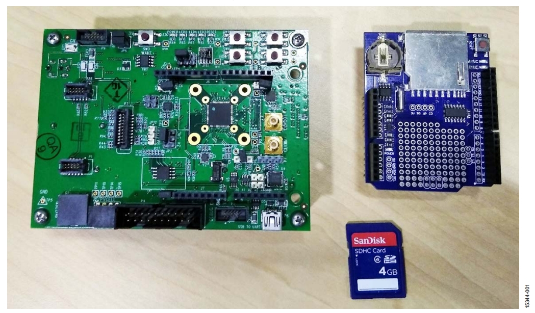
The hardware used to demonstrate interfacing between the SD card and the ADuCM3027/ADuCM3029 processor is as follows:
- The EVAL-ADuCM3029 EZ-KIT® board
- Arduino®-compatible data logging shield
- 4 GB SanDisk® SD card
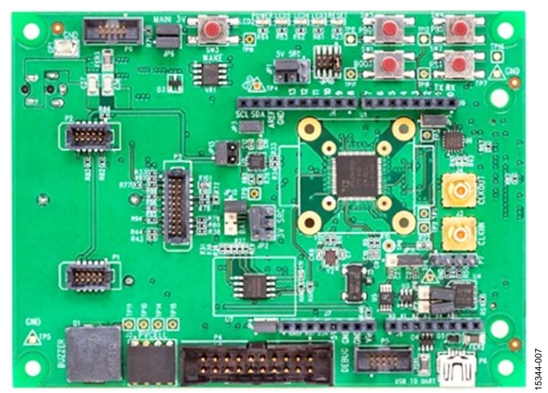
EVAL-ADuCM3029 EZ-KIT Board
The EVAL-ADuCM3029 EZ-KIT board is an evaluation system for the ADuCM3027/ADuCM3029 processor (see Figure 7). The board contains a wide array of on-board components that can evaluate the ADuCM3027/ADuCM3029 microcontroller. The EVAL-ADuCM3029 EZ-KIT also contains an EI3 interface and an Arduino interface. These interfaces provide connectivity with various daughter boards and shields to expand the functionality of the EVAL-ADuCM3029 EZ-KIT board.

Arduino-Compatible Data Logging Shield
The data logging shield used is a commonly used shield in most Arduino logging projects (see Figure 8). The SPI of the logging shield connects with the SPIH port of the ADuCM3027/ ADuCM3029 microcontroller.

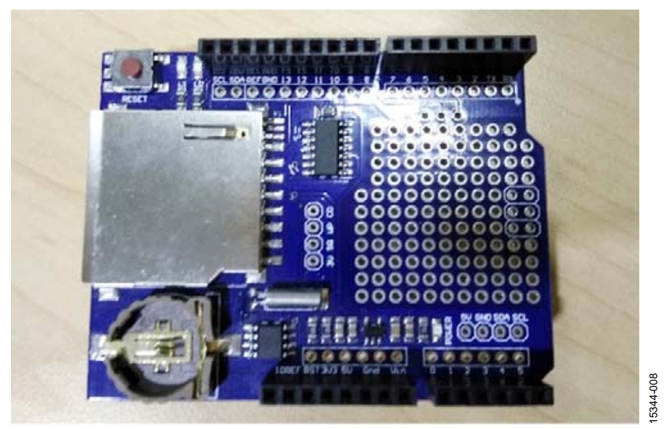
Most of the data logging shields include a complementary metal-oxide semiconductor (CMOS) buffer (for example, the CD4050) that acts as a 3.3 V to 5 V voltage translator and protects the SD card from damage. Usually the data in, serial clock, and chip select lines of the SD card are buffered because these are input pins of the card. However, when interfacing an SD card with the ADuCM3027/ADuCM3029 microcontroller, this voltage translator is optional because the output of the microcontroller has the same voltage level as the SD cards.
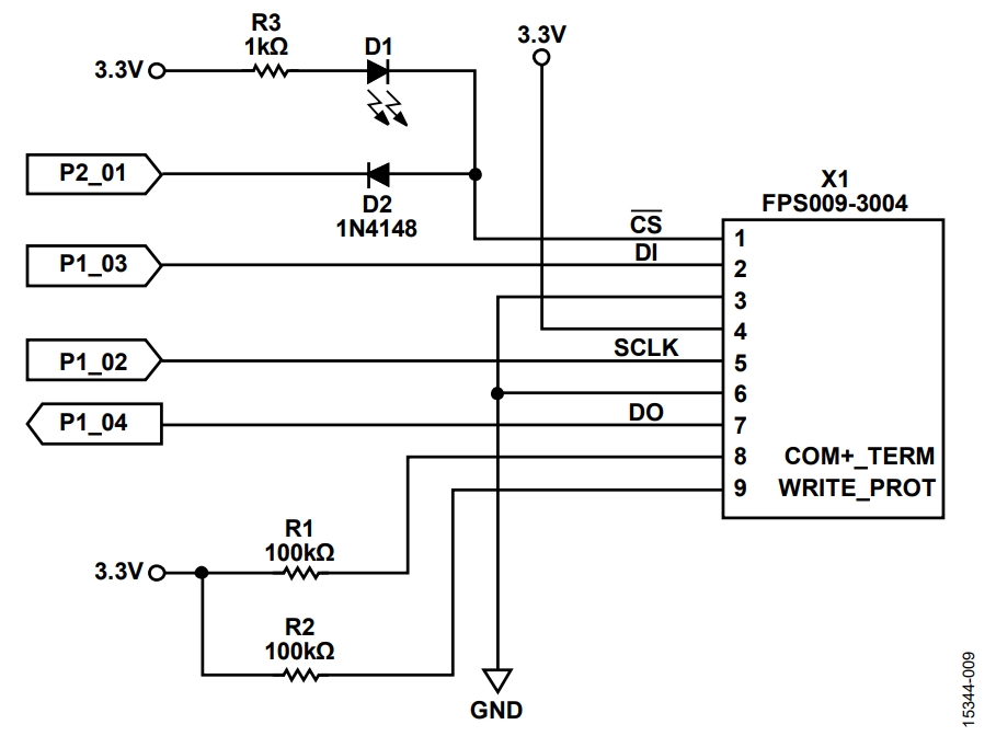
The SPIH interface and general-purpose input/output (GPIO) Port 1 share the pins of the ADuCM3027/ADuCM3029 microcontroller. The SPIH, SCLK, MOSI, and MISO signal lines also use the microcontroller pins (Pin P1_02, Pin P1_03, and Pin P1_04); therefore, these pins must remain unused.
For this application note, this application uses GPIO Pin P2_01 as chip select for the SD card, and the SPIH dedicated chip selects are not used (see Figure 9).

Software Implementation
To test this application, use the following software tools:
- IAR Embedded Workbench 7.60. See the EVAL-ADuCM3029 EZ-KIT page for to download this software.
- ADuCM302x Software for IAR, available for download from the EVAL-ADuCM3029 EZ-Kit page.
- The FatFs library R0.12a by ChaN, available from the FatFs - Generic FAT Filesystem Module website.
The application uses the FatFs library that handles the file system calls and enables to reading and modifying files in the FAT-formatted SD card. To use this file system library, a hardware abstraction layer must be implemented that handles the low level hardware dependent functions calls.
SPI Interface Initialization
To initialize the ADuCM3027/ADuCM3029 SPIH peripheral, take the following steps:
- Configure the SPIH peripheral.
- Configure the GPIO Pin P2_01 as the chip select.
- Configure the pin multiplexing for the shared pins of GPIO1 and SPIH.
Configuring the SPIH Peripheral
The SPIH peripheral configuration consists of calls to set the SPIH peripheral into a ready state for communication with the SD card. To configure the SPIH peripheral, take the following steps:
- Open the SPIH peripheral.
- Set the bit rate. Note that the SPIH bit rate changes depend
on what the interaction of the microcontroller and the SD
card is:
- When the microcontroller is initializing the SD card for communication, the bit rate must be between 100 kHz to 400 kHz.
- After configuration of SD card in SPI mode, the bit rate can be as high as 20 MHz depending on the design of the hardware and capacity of the microcontroller
- Set for continuous mode operation. In continuous mode, the SPI peripheral can perform multiple byte transmit and receive without cancelling or interrupting the transfer.
The following is a sample of the code used to configure the SPIH of the ADuCM3027/ADuCM3029 microcontroller:
static uint8_t SPIMem[ADI_SPI_MEMORY_SIZE];
static ADI_SPI_HANDLE spih_Dev;

// Open the SPI
adi_spi_Open(SPI_DEV_NUM, SPIMem,
ADI_SPI_MEMORY_SIZE,
&spih_Dev);

// Set the bit rate
adi_spi_SetBitrate(spih_Dev, 100000);

// Set the continuous mode
adi_spi_SetContinousMode(spih_Dev, true);
Configuring the Chip Select
The chip select uses a GPIO pin (Pin P2_01) instead of using the SPI dedicated chip selects. Using the customized GPIO pin gives the user full control of the chip select signal. Some of the transactions between the SD card and the microcontroller need special handling of the chip select signal so that the software controls the chip select appropriately
To configure the chip select pin, set the SPIH chip select option to none, then configure the GPIO Pin P2_01 as an output by using the following:
adi_spi_SetChipSelect (spih_Dev,
 ADI_SPI_CS_NONE);
adi_gpio_OutputEnable (SPI_CS_PORT,
SPI_CS_PIN,
 true);
adi_gpio_SetHigh(SPI_CS_PORT, SPI_CS_PIN);
Configuring the Microcontroller Pin Multiplexers
The GPIOx_CFG register is the configuration register that holds the settings of the pin multiplexers of the ADuCM3027/ ADuCM3029 microcontroller. SPIH uses the Pin P1_02, Pin P1_03, and Pin P1_04 as connection pins to the SD card.
To configure the pins for SPIH usage, set the proper bit options in the REG_GPIO1_CFG register. For more information on this register, see the ADuCM302x Ultra Low Power ARM Cortex-M3 MCU with Integrated Power Management Hardware Reference manual.
The following code is a sample for setting the port configuration register for SPIH use:
#define SPI0_SCLK_PORTP1_MUX
((uint32_t) ((uint32_t) 1<<4))
#define SPI0_MISO_PORTP1_MUX
((uint32_t) ((uint32_t) 1<<8))
#define SPI0_MOSI_PORTP1_MUX
((uint32_t) ((uint32_t) 1<<6))


*((volatile uint32_t *) REG_GPIO1_CFG) =
SPI0_SCLK_PORTP1_MUX |
SPI0_MISO_PORTP1_MUX |
SPI0_MOSI_PORTP1_MUX;
Sending and Receiving Data
After configuring the SPI peripheral for SD card communications, the interface is now ready for sending and receiving data packets and SD card initiation. The adi_spi_ReadWrite function sends and receives data from the SD card. This function requires a structure instruction that holds the data and the SPI device pointer. The following is a sample of the code described in this section:
ADI_SPI_TRANSCEIVER spi_xcv_buff;
spi_xcv_buff.pTransmitter = txbuff;
spi_xcv_buff.pReceiver = rxbuff;
spi_xcv_buff.TransmitterBytes = txsize;
spi_xcv_buff.ReceiverBytes = rxsize;
spi_xcv_buff.nTxIncrement = 1;
spi_xcv_buff.nRxIncrement = 1;

adi_spi_ReadWrite(spih_Dev, &spi_xcv_buff);
The ADI_SPI_TRANSCEIVER is a structure instruction that holds the buffers used in the transaction. The buffers for transmission, reception, data sizes, and increments must be defined.
Transmission and reception buffers are uint8_t arrays with sizes that are in accordance with the data that is transmitted or received. For transmission, the data size is approximately 6 bytes to 8 bytes, and the reception data size is from 1 byte to 512 bytes.
Note that the adi_spi_ReadWrite function is a blocking function, and the microcontroller waits until the transaction is successful to execute the next instruction.
Sample Code for SD Card Microcontroller Interfacing
This application note has an accompanied sample code for SD card to ADuCM3027/ADuCM3029 interfacing. To view the sample code, decompress and import the project to the IAR Embedded Workbench 7.6, available for download from the EVAL-ADuCM3029 EZ-KIT product page.
References
ADuCM302x Ultra Low Power ARM Cortex-M3 MCU with Integrated Power Management Hardware Reference. Analog Devices, Inc. 2016.
SD Specifications Part 1, Physical Layer Simplified Specifications, Version 5.00. SD Card Association. 2014.