引言
本文的第一部分介绍了文氏电桥振荡器的发展历程与工作原理,并结合理想电路元件开展了仿真分析。第二部分将聚焦实用文氏电桥振荡器的分析与制作,并对其性能进行测量。作为补充内容,我们还将制作并测试一款性能显著更优的备选电路。
文后附有印刷电路板(PCB)设计文件链接,方便读者在阅读过程中自行制作电路板。
完整实用文氏电桥振荡器的仿真与构建
我们非正式地讨论过利用灯泡作为增益控制元件。虽然这种方案确实可行,但别想随便拿个灯泡就让电路正常工作,灯泡必须精心挑选。下面,我们首先探讨一种实现方案,它利用反并联二极管来温和地控制放大器的增益。
材料
- ADALM2000 (M2K)主动学习模块或:
- 双通道示波器、信号发生器和/或网络分析仪功能
- ±5 V双极性跟踪电源
- ADALP2000套件明细:
- 无焊试验板
- 跳线套件
- 两个10 nF电容
- 两个1 µF电容
- 三个10 kΩ电阻
- 两个4.7 kΩ电阻
- 一个5 kΩ单圈电位计
- 两个1N4148硅二极管
此外,我们提供了PCB文件和匹配的LTspice®仿真文件,可用于制作此实验所用的PCB,详见文后的 文氏电桥PCB文件和LTspice文件。
图1所示电路是一款完整(且实用)的文氏电桥振荡器电路,可在试验板上构建。该电路没有使用白炽灯泡(其有效电阻随着所施加电压的提高而增大)作为放大器的输入电阻,而是将二极管与部分反馈电阻并联,使其有效电阻随着所施加电压的提高而减小。如果忽略二极管,增益将为1 + (10k + 4.7k)/(4.7k + 2k), 即大约3.19(须知,理想文氏电桥需要3.0的增益才能维持振荡)。但是,当D1和D2两端的电压达到600 mV左右时,D1、D2和R2并联组合的电阻会减小,导致增益降低。


在LTspice中打开wien_bridge_osc_complete.asc,然后运行仿真。输出应与图2中的仿真结果类似。仿真开始后,V3激励电路会立即向电桥施加0.1 V、5 ms的脉冲。该激励电路对于启动仿真而言并非必需,但它有助于仿真更快达到稳态。若没有该激励电路,仿真最终仍会开始,但模型中放大器的低失调可能会引起显著的延迟。在一些实际应用中,启动时间也是一个问题。为此,可以采用类似于V3的电路,例如由逻辑门构成的脉冲发生器。请使用不同的vkick值(包括0)进行实验。

接下来,按照图3所示构建电路。


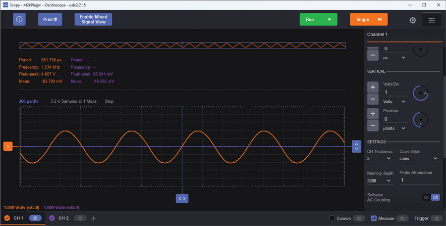
请注意,R5是一个电位计,通过调节它可将电路增益设定到振荡开始的临界值。利用Scopy的示波器来测量输出;将垂直刻度设置为1 V/div,并将时基设置为200 µs/div。结果应与图4类似。

这个正弦波看起来很完美,但其完美程度究竟如何呢?能否用 肉眼发现其中的任何失真?在时域(示波器)图中,肉眼几乎 无法察觉到失真。即使与完美的参考正弦波进行比较,小于1% 的失真也很难被观察到。要真正分析低水平的失真分量,必须 使用傅里叶变换技术,而这正是Scopy频谱分析仪的核心功能。 打开频谱分析仪,将将起始频率(Start frequency)设置为0 kHz,停止频率(Stop frequency)设置为20 kHz, ,顶部(Top)设置为0 dB, 底部(Bottom)设置为-120 dB。重要提示:点击通道1 (Channel 1)设置,选择Blackman-Harris窗口,并将增益模式(Gain Mode)设置为高(High)。
注:
ADALM2000有两种输入量程:±2.5 V和±25 V。在示波器模式下,当 调整垂直增益时,系统会自动选择量程,但在频谱分析仪模式 下,量程不会自动选择。如果将振荡器的增益提高到输出超过 ±2.5 V的程度,则需要将增益模式(Gain Mode)设置为低(Low)以避免削波。削波虽然不会损坏任何硬件,但会引发严重失真。
观察振荡器输出的频谱,如图5所示。

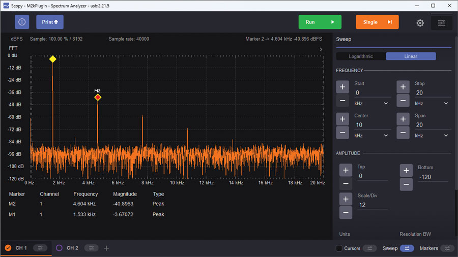
虽然使用二极管箝位来限制增益的方法很简单,但很难将失真控制在优于约–40 dB(即1%)的水平。
问题
1. 增益控制元件与失真之间有何关系?
2. 如果将二极管箝位电路中的一个二极管替换为肖特基二极管(其正向压降低于硅二极管),失真分量(谐波)会发生什么变化?
失真大幅降低的改进版电路
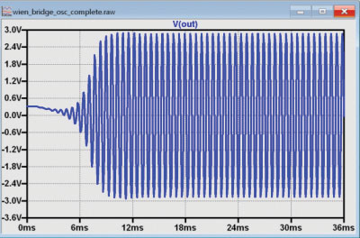
下面,我们来对本系列第一部分的图1电路进行改进。#327白炽灯泡是一个28 V指示灯,其冷态电阻约为130 Ω,热态电阻约为650 Ω。在LTspice中,可将该灯泡建模为一个电阻元件,其阻值是功耗的函数。然而,该阻值不能瞬间改变,如果该阻值能瞬间改变,当输出正弦波从零上升到最大幅度、再回落到零并转向最大负幅度的时侯,放大器的增益也会随之同步改变,导致输出波形出现失真,而这显然不是我们想要的。
电路的运行要求灯泡的热时间常数远大于输出周期的一半。为什么要以输出周期的一半为参照?回想一下,电阻功耗的计算公式为V2/r,故正负输出摆幅均会产生正功耗。为了模拟这一时间滞后,可将灯泡的功耗转换为电流,此电流驱动一个并联R-C网络(R100和C100),其时间常数为50 ms,远大于1.59 kHz输出的半周期628 µs。因此,灯泡的电阻取决于多个周期的平均功耗。
打开wien_bridge_osc_experimenter.asc 仿真文件,如图6所示。请注 意,此仿真文件位于“PCB设计文件”文件夹中。


运行仿真并探测输出,如图7所示。

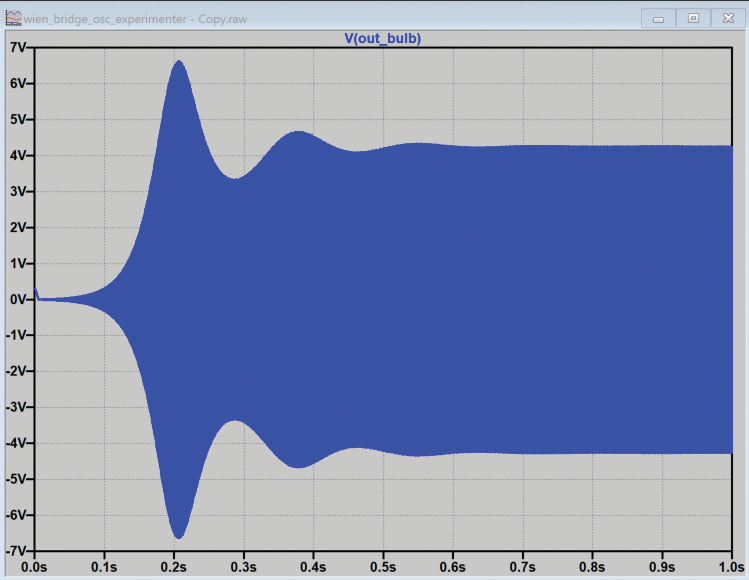
注意初始瞬态,此时电路正在寻找恰当的幅度以维持振荡。虽然该电路可在试验板上搭建,但鉴于已进展到这一步,不妨制作一个更可靠、能长期使用的版本。图8展示了连上ADALM2000的完整PCB。

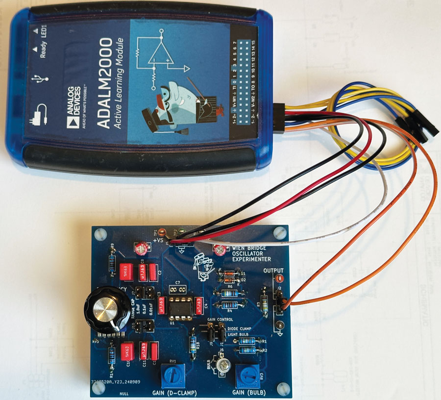
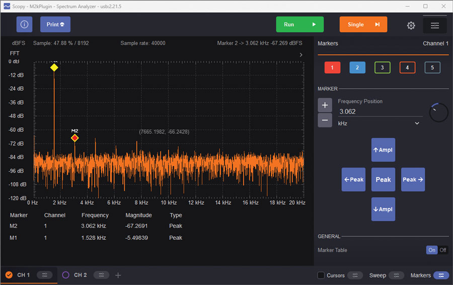
图9显示了设置为灯泡控制的文氏电桥振荡器实验板的输出频谱。请注意,三次谐波优于-60 dB(即0.01%),比二极管箝位电路通常可实现的失真水平低一个数量级。事实上,该指标已逼近ADALM2000本身的失真下限!测量领域有一个公认原则:测量仪器本身的精度应优于被测设备4到10倍(具体倍数因情况而异)。我们已触及ADALM2000的测量极限。若要对该电路的失真进行更准确可靠的测量,必须采用性能更好的测试仪器。

结语
第一部分重点介绍了文氏电桥振荡器的背景和原理,第二部分则结合一个动手制作练习,详细探讨了实际实现方法,以加深读者的理解。现在,您手里有一个高性能振荡器,其工作原理您已了然于心。接下来该如何使用它呢?不妨将旧饼干罐改造为仪器外壳,挑选几个别致的控制旋钮,再从杂物箱中找到电源开关,做出一台独一无二的测试设备,定能让亲朋好友和同事眼前一亮。
问题
3. 在音频领域,失真测量仪器的技术已发展到什么程度?
4. 如果负担不起最先进的台式失真分析仪,是否还有其他选择?(提示:观看本系列第一部分中的视频!)
您可以在学子专区论坛上找到问题答案。
参考电路
Bill Hewlett,“A New Type Resistance-Capacity Oscillator”(硕士论文),kennethkuhn.com,2020年5月。
“Using Lamps for Stabilizing Oscillators”,Tronola,2011年10月。
Wien Bridge Oscillator(文氏电桥振荡器),维基百科。
Jim Williams,“应用笔记43:桥接电路——兼顾增益与平衡”, 凌力尔特,1990年6月。
Jim Williams,“TThank You, Bill Hewlett.”,EDN杂志,2001年2月。
Jim Williams和Guy Hoover,“应用笔记132:A-D转换器保真度测试”,凌力尔特,2011年2月。
致谢
本次实验的灵感源于ASEE 2022会议上与《EE Freshman Practicum》一 书的作者Robert Bowman博士合作举办的研讨会。该研讨会的完整视频可在YouTube上观看。
