AD9410
PRODUCTION10-Bit, 210 MSPS ADC
- Part Models
- 1
- 1ku List Price
- Starting From $80.75
Overview
- SNR = 54 dB with 99 MHz analog input
- 500 MHz analog bandwidth
- On-chip reference and track and hold
- 1.5 V p-p differential analog input range
- 5.0 V and 3.3 V supply operation
- 3.3 V CMOS/TTL outputs
- Power: 2.1 W typical at 210 MSPS
- Demultiplexed outputs each at 105 MSPS
- Output data format option
- Data sync input and data clock output provided
- Interleaved or parallel data output option
The AD9410 is a 10-bit monolithic sampling analog-to-digital converter (ADC) with an on-chip track-and-hold circuit and is optimized for high speed conversion and ease of use. The product operates at a 210 MSPS conversion rate, with outstanding dynamic performance over its full operating range.
The ADC requires a 5.0 V and 3.3 V power supply and up to a 210 MHz differential clock input for full performance operation. No external reference or driver components are required for many applications. The digital outputs are TTL-/CMOS-compatible and separate output power supply pins also support interfacing with 3.3 V logic.
The clock input is differential and TTL-/CMOS-compatible. The 10-bit digital outputs can be operated from 3.3 V (2.5 V to 3.6 V) supplies. Two output buses support demultiplexed data up to 105 MSPS rates and binary or twos complement output coding format is available. A data sync function is provided for timing-dependent applications. An output clock simplifies interfacing to external logic. The output data bus timing is selectable for parallel or interleaved mode, allowing for flexibility in latching output data.
Fabricated on an advanced BiCMOS process, the AD9410 is available in an 80-lead thin quad flat package, exposed pad specified over the industrial temperature range (−40°C to +85°C).
PRODUCT HIGHLIGHTS
- High Resolution at High Speed—The architecture is specifically designed to support conversion up to 210 MSPS with outstanding dynamic performance.
- Demultiplexed Output—Output data is decimated by two and provided on two data ports for ease of data transport.
- Output Data Clock—The AD9410 provides an output data clock synchronous with the output data, simplifying the timing between data and other logic.
- Data Synchronization—A DS input is provided to allow for synchronization of two or more AD9410s in a system, or to synchronize data to a specific output port in a single AD9410 system.
APPLICATIONS
- Communications and radars
- Local multipoint distribution services (LMDS)
- High-end imaging systems and projectors
- Cable reverse paths
- Point-to-point radio links
Documentation
Data Sheet 1
Application Note 6
Technical Articles 4
Evaluation Design File 1
ADI has always placed the highest emphasis on delivering products that meet the maximum levels of quality and reliability. We achieve this by incorporating quality and reliability checks in every scope of product and process design, and in the manufacturing process as well. "Zero defects" for shipped products is always our goal. View our quality and reliability program and certifications for more information.
| Part Model | Pin/Package Drawing | Documentation | CAD Symbols, Footprints, and 3D Models |
|---|---|---|---|
| AD9410BSVZ | 80-Lead TQFP (14mm x 14mm w/ EP) |
| Part Models | Product Lifecycle | PCN |
|---|---|---|
|
Mar 15, 2016 - 14_0258 Assembly Transfer of Selected 14x14 LQFP, 14x14 LQFP_EP and 7x7,10x10,12x12,14x14 TQFP_EP Products to Amkor Philippines |
||
| AD9410BSVZ | PRODUCTION | |
|
Oct 28, 2009 - 08_0008 Qualification of 8" 0.6um BiCMOS wafer fab process at Analog Devices, Limerick, Ireland. |
||
| AD9410BSVZ | PRODUCTION | |
|
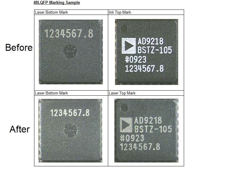
Jun 16, 2009 - 09_0027 Conversion to Laser Mark for the LQFP Packages (Single Grades) |
||
| AD9410BSVZ | PRODUCTION | |
This is the most up-to-date revision of the Data Sheet.
Software Resources
Can't find the software or driver you need?
Request a Driver/SoftwareTools & Simulations
AD9410 IBIS Models 1
Latest Discussions
No discussions on AD9410 yet. Have something to say?
Start a Discussion on EngineerZone®