AN-1577: Variable Gain Noninverting Amplifier Using the AD5292 Digital Potentiometer and the OP184 Op Amp
Circuit Function and Benefits
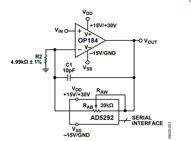
This circuit provides a low cost, high voltage, variable gain noninverting amplifier using the AD5292 digital potentiometer in conjunction with the OP184 operational amplifier (op amp).

(Decoupling and All Connections Not Shown)
The circuit offers 1024 different gains that can be controlled through a serial peripheral interface (SPI) compatible, serial digital interface. The ±1% resistor tolerance performance of the AD5292 provides low gain error over the full resistor range, as shown in Figure 2.


The circuit supports rail-to-rail inputs and outputs for single-supply operation at +30 V and dual-supply operation at ±15 V, and is capable of delivering up to ±6.5 mA of output current.
In addition, the AD5292 has an internal 20× programmable memory that allows a customized gain setting at power-up.
The circuit provides accuracy, low noise, and low total harmonic distortion (THD) and is suited for signal instrumentation conditioning.
Circuit Description
The circuit employs the AD5292 digital potentiometer in conjunction with the OP184 operational amplifier, which provides a low cost, variable gain noninverting amplifier.
The input signal, VIN, is amplified by the OP184. The op amp offers low noise, high slew rate, and rail-to-rail inputs and outputs.
The maximum circuit gain (G) is defined in by the following equation:

where:
RAB is the resistance from Terminal A to Terminal B of the AD5292.
The maximum current through the AD5292 is ±3 mA, which limits the maximum input voltage, VIN, based on the circuit gain as described in Equation 2.

When the input signal connected to VIN is higher than the theoretical maximum value from Equation 2, increase R2 and the new gain can be recalculated using Equation 1.
The ±1% internal resistor tolerance of the AD5292 ensures a low gain error, as shown in Figure 2.
The circuit gain equation is as follows:

where D is the code loaded in the digital potentiometer.
When the circuit input is an ac signal, the parasitic capacitances of the digital potentiometer can cause undesirable oscillation in the output. Avoid this oscillation by connecting a small capacitor, C1, between the inverter input and its output. A value of 10 pF was used for the gain and phase plot shown in Figure 3.


A modification of the circuit provides a logarithmic gain function, as shown in Figure 4. In this case, the digital potentiometer is configured in the ratiometric mode.


The circuit gain is defined in Equation 4.

A gain plot vs. code is shown in Figure 5.


The AD5292 has a 20× programmable memory, which allows presetting the output voltage in a specific value at power-up.
Excellent layout, grounding, and decoupling techniques must be utilized in order to achieve the desired performance from the circuits discussed in this application note (see Tutorial MT-031, Grounding Data Converters and Solving the Mystery of “AGND” and “DGND” and Tutorial MT-101, Decoupling Techniques). As a minimum, use a 4-layer printed circuit board (PCB) with one ground plane layer, one power plane layer, and two signal layers.
Common Variations
The AD5291 (8 bits with 20× programmable power-up memory) and the AD5293 (10 bits with no power-up memory) are ±1% tolerance digital potentiometers that are suitable for this application.
References
MT-032 Tutorial, Ideal Voltage Feedback (VFB) Op Amp, Analog Devices.
MT-087 Tutorial, Voltage References, Analog Devices.