AN-1575: Single-Ended to Differential High Speed Drive Circuit for the AD7626 16-Bit,10 MSPS ADC
Circuit Function and Benefits
The circuit shown in Figure 1 provides a method to convert a high frequency, single-ended input signal to a balanced differential signal that is used to drive the AD7626 16-bit, 10 MSPS, PulSAR® analog-to-digital converter (ADC). The circuit maximizes the AD7626 performance for high frequency input tones using the ADA4932-1 low power differential amplifier to drive the ADC. The benefit of this combination of devices is high performance at low power.

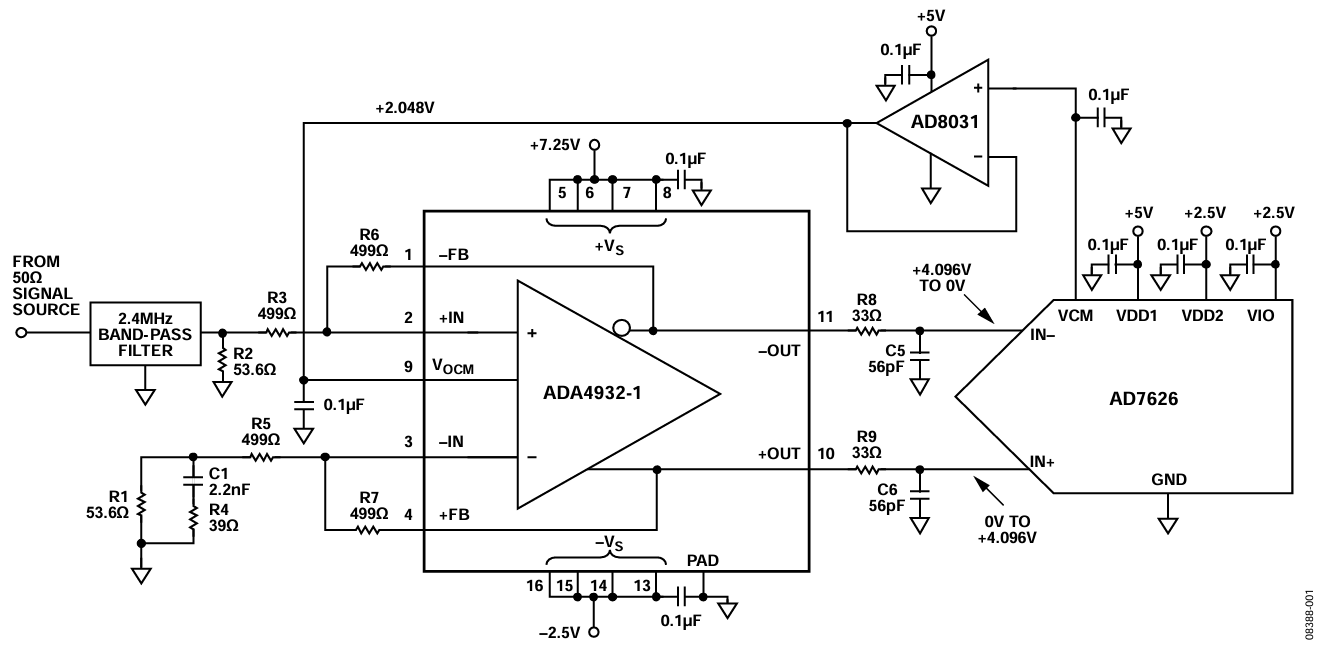
Figure 1. ADA4932-1 driving the AD7626 (all connections and decoupling not shown).
The AD7626 dynamic performance of 91.5 dB signal-to-noise ratio (SNR) at 10 MSPS with ±0.45 LSB integral nonlinearity (INL) performance, no latency, and low voltage differential signaling (LVDS) interface, coupled with power dissipation of 136 mW. The successive approximation register (SAR) architecture used in the AD7626 can sample at 10 MSPS without latency that is also known as pipeline delay, which is typically incurred with pipeline ADCs.
The ADA4932-1 has low distortion (100 dB spurious-free dynamic range (SFDR) at 10 MHz), fast settling time (9 ns to 0.1%), high bandwidth (560 MHz, −3 dB, G = 1), and quiescent current (9.6 mA). These characteristics make the ADA4932-1 the an ideal choice for driving the AD7626. The ADA4932-1 also features the functionality to set the required output common-mode voltage.
The combination of the ADA4932-1 and the AD7626 offers dynamic performance and small board area with the AD7626 in a 5 mm × 5 mm, 32-lead LFCSP, the ADA4932-1 in a 3 mm × 3 mm, 16-lead LFCSP, and the AD8031 in a 5-lead SOT-23 package.
Circuit Description
Using a differential amplifier to drive an ADC successfully is linked to balancing each side of the differential amplifier correctly. Figure 1 shows the schematic for the ADA4932-1, AD7626, AD8031, and associated circuitry. In the test circuit used, the signal source is followed by a 2.4 MHz band-pass filter. The band-pass filter eliminates the harmonics of the 2.4 MHz signal and ensures that only the frequency of interest is passed to and processed by the ADA4932-1 and AD7626.
The signal source in this case has a characteristic impedance of 50 Ω and is ac-coupled to the ADA4932-1 via the band-pass filter. Applying the signal source to the positive input of the ADA4932-1 requires that the source properly terminates at 50 Ω as well, or in general, whatever the source impedance is. The termination resistor, R2, is selected such that the parallel combination of R2 and the input impedance (RIN) of the ADA4932-1 is equal to 50 Ω.
To calculate the input impedance of the ADA4932-1 (looking into the R3 resistor), use the following equation:
where:
RG is the gain resistor. RG = R3 = R5 = 499 Ω.
RF is the feedback resistor. RF = R6 = R7 = 499 Ω.
For these values, the input impedance of this circuit is approximately 665 Ω. The 665 Ω input impedance of the ADA4932-1, in parallel with the 53.6 Ω resistor (R2), is equal to 50 Ω, that is, the input source impedance.
To maintain proper balance and symmetry between the two inputs of the ADA4932-1, the equivalent Thevenin impedance of the input source impedance and termination must be added to the inverting input. In this case, this involves the ac characteristics of the filter.
The Thevenin equivalent network is shown on the inverting input (IN−) of the ADA4932-1 in Figure 1. This circuit is optimized for performance at 2.4 MHz. The R1 resistor is paralleled by the series combination of C1 and R4. At 2.4 MHz, the complex series combination of C1 and R4 equals 55.6 Ω. The 55.6 Ω impedance in parallel with R1 is within a few ohms of the Thevenin equivalent circuit input impedance on the non-inverting input. Matching of the two inputs ensures that the outputs are symmetrical, balanced, and optimized for lowest distortion.
For a more detailed explanation of how to terminate a single-ended input, refer to the ADA4932-1 data sheet or Application Note AN-1026, High Speed Differential ADC Driver Design Considerations. The ADI DiffAmpCalculator™ Design Tool simplifies this termination and provides keen insight to other differential amplifier design related issues.
The ADA4932-1 differential driver is configured in a gain of approximately 1 (single-ended input to differential output). Because of the 50 Ω signal source and the termination matching at the ADA4932-1 input, the net overall gain of the channel is approximately 0.5 with respect to the Thevenin equivalent signal source voltage.
The common-mode voltage at the output of the ADA4932-1 is set by buffering the VCM pin output voltage (nominally 2.048 V) from the AD7626 with the AD8031 configured as a unity-gain buffer. The AD8031 provides the ADA4932-1 VOCM pin with a low source impedance and is capable of driving the large bypass capacitor, as shown in Figure 1.
The ADA4932-1 is particularly useful when driving higher frequency inputs to the AD7626, a 10 MSPS ADC with a switched capacitor input. The resistor (R8 and R9) and capacitor (C5 and C6) circuit between IN+ and IN− pins of the ADA4932-1 and AD7626 acts as a low-pass filter to noise. The filter limits the input bandwidth to the AD7626, but the main function of the filter is to optimize the interface between the driving amplifier and the AD7626. The series resistor isolates the driver amplifier from high frequency switching spikes from the ADC switched capacitor front-end. The AD7626 data sheet shows values of 20 Ω and 56 pF. In the circuit shown in Figure 1 these values were empirically optimized to 33 Ω and 56 pF. The resistor capacitor (RC) combination can be optimized slightly for the circuit and input frequency being converted by simply varying the RC combination. Note that the incorrect RC combination limits the total harmonic distortion (THD) and linearity performance of the AD7626. Increasing the bandwidth as seen by the ADC introduces more noise.
Another aspect of optimization is the selection of the power supply voltages for the ADA4932-1. In the circuit, the output common-mode voltage (VCM pin) of the AD7626 is 2.048 V for the internal reference voltage of 4.096 V, and each input pin (IN+ and IN−) swings between 0 V and 4.096 V, 180° out of phase. This provides an 8.2 V full-scale differential input to the ADC. The ADA4932-1 output stage requires about 1.4 V of headroom with respect to each supply voltage for linear operation. Optimal distortion performance is obtained when the supply voltages are approximately symmetrical around the common mode voltage. If a negative supply of −2.5 V is chosen, a positive supply of at least +6.5 V is required for symmetry around the common-mode voltage of 2.048 V.
Testing results indicate that a positive supply of 7.25 V gives the best overall distortion for a 2.4 MHz tone.
Using a low jitter clock source and a single tone, −1 dBFS amplitude, 2.402 MHz input to the AD7626 yields the fast Fourier transform (FFT) results shown in Figure 2 (88.49 dB of SNR and −86.17 dBc of THD). Figure 2 shows that the harmonics of the fundamental alias back into the pass band. For example, when sampling at 10 MSPS, the third harmonic (7.206 MHz) aliases into the pass band at 10.000 MHz – 7.206 MHz = 2.794 MHz. Figure 3 shows a FFT plot for a tone with an amplitude of −6 dBFS.

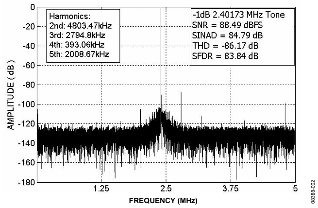
Figure 2. AD7626 output, 64,000 point, FFT plot, −1 dBFS amplitude, 2.40173 MHz input ton,10.000 MSPS sampling rate.

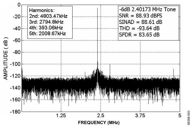
Figure 3. AD7626 output, 64,000-point FFT plot, −6 dBFS amplitude, 2.40173 MHz input tone, 10.000 MSPS sampling rate.
The nonharmonic noise admitted through the pass band of the band-pass filter used in the circuit is replaced by the average noise across the Nyquist bandwidth when calculating the SNR and THD.
The performance of this or any high-speed circuit is highly dependent on proper printed circuit board (PCB) layout. This includes, but is not limited to, power supply bypassing, controlled impedance lines (where required), component placement, signal routing, and power and ground planes. See MT-031 Tutorial, MT-101 Tutorial and the technical article A Practical Guide to High-Speed Printed-Circuit-Board Layout for more details.
Typical Connections and Reference Configurations of the AD7626
The typical connection diagram for the AD7626 is shown in Figure 4. The AD7626 has an integrated internal reference, as well as two provisions for external references if required by the system. The reference voltage can be generated by applying the ADR280 reference (1.2 V) output to the REFIN pin of the AD7626, which is amplified internally by the on-chip reference buffer to the correct ADC reference value of 4.096 V. The ADR280 can be supplied by the same 5 V analog rail used for the AD7626 and make use of the on-chip reference buffer. Alternatively, a 4.096 V external reference (ADR434 or ADR444) can be applied to the unbuffered REF input of the AD7626. This approach is common for multichannel applications where the system reference is typically buffered discretely (using an AD8031) and is shared by all ADC channels. The ADR434 and the ADR444 configurations are also ideal for single-channel applications where a low reference temperature coefficient (3 ppm/°C max for ADR434B and ADR444B) is required. The positive rail that is used to supply the ADA4932-1 amplifier can also supply the VIN supply pin of the ADR434 or the ADR444.

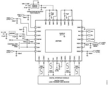
Figure 4. Typical connection diagram for AD7626 showing decoupling and LVDS interface connections.
Common Variations
This circuit operates with good stability and accuracy with the component values shown. This circuit is dc-coupled; however, another common application is ac coupling. Common variations to this circuit include a single-supply voltage, inputs that are driven differentially, and inputs that require attenuation of the signal. Other ADC drivers/differential amplifiers can also be used to tailor the performance to the application, for example, power, noise, bandwidth, and architecture.