AN-1559: Migrating to the AD7606B from the AD7606
Introduction
The AD7606B is an enhanced version of the AD7606 analog-to-digital, data acquisition systems (DAS). The AD7606B is a pin for pin replacement for the AD7606 with no hardware modifications required to the existing designs, with the following improved features:
- Higher input impedance (RIN), 5 MΩ typical, with lower temperature drift.
- Faster throughput rate of up to 800 kSPS.
- Extended operating temperature range up to 125°C.
- Lower digital supply (VDRIVE) range down to 1.71 V.
- Higher clamp voltage up to ±21 V.
This application note describes the differences between the hardware mode of the AD7606 and the AD7606B.
For full details on the AD7606 and the AD7606B, see the AD7606 data sheet and the AD7606B data sheet, which should be consulted in conjunction with this application note.
Hardware Compatibilty
The AD7606B is a pin for pin replacement for the AD7606, with no hardware modifications required on existing designs. The functionality of some of the pins have changed to enable the software mode capability on the AD7606B. The pin functionality differences are detailed in Table 1.
| Pin No. | AD7606 Mnemonic | AD7606B Mnemonic |
| 3 | OS 0 | OS01 |
| 4 | OS 1 | OS11 |
| 5 | OS 2 | OS21 |
| 6 | PAR/SER/BYTE SEL | PAR/SER SEL |
| 10 | CONVST B | WR2 |
| 27 | DB9 | DB9/DOUTC2 |
| 28 | DB10 | DB10/DOUTD2 |
| 29 | DB11 | DB11/SDI2 |
| 32 | DB14/HBEN | DB14 |
| 33 | DB15/BYTE SEL | DB15 |
| 1 Pulling the OS0, OS1, and OS2 pins high sets the AD7606B to software mode. This combination is invalid on the AD7606. 2 Only applicable when using software mode. |
||
Pin 10 and Pin 9 Differences
Pin 10 (CONVST B) in the AD7606 is the CONVSTB input that initiates conversions on Channel 5 to Channel 8, and Pin 9 (CONVST A) in the AD7606 is the CONVST A input that initiates conversions on Channel 1 to Channel 4. In the AD7606B, Pin 9 (CONVST) is the CONVST input for all eight channels. In the AD7606B, Pin 10 (WR) is the write input for writing registers to software parallel mode. When not using software parallel mode for the AD7606B, tie WR high, low, or to the CONVST pin.
Pin 6, Pin 32, and Pin 33 Differences
Use Pin 6 (PAR/SER/BYTE SEL) of the AD7606 to select the serial, parallel, or parallel byte interface. The AD7606B does not support the parallel byte interface. Therefore, Pin 6 (PAR/SER SEL) of the AD7606B can only select between a serial or parallel interface. In addition, when using a parallel interface, the only function available for Pin 33 of the AD7606B is DB15, and the only function available for Pin 32 of the AD7606B is DB14. If using a serial interface, tie Pin 32 and Pin 33 of the AD7606B to AGND.
Pin 27, Pin 28, and Pin 29 Differences
In the AD7606, Pin 27 (DB9), Pin 28 (DB10), and Pin 29 (DB11) are parallel data output lines. When using hardware mode for the AD7606B, these pins are also the parallel data output lines.
When using software mode for the AD7606B, the serial interface can be configured to have four output data lines. Therefore, two extra serial data outputs, DOUTC and DOUTD, can be enabled on Pin 27 and Pin 28 of the AD7606B.
In software mode, Pin 29 of the AD7606B is the serial data input (SDI) used to write registers in the memory map. See Table 3 for the pin functionality for each device and operating mode.
Power Supplies
The analog power supply voltage range (AVCC) in the AD7606B is the same as the AD7606 (4.75 V to 5.25 V). The logic supply voltage range (VDRIVE) in the AD7606 is 2.3 V to 5.25 V, whereas the logic supply voltage range in the AD7606B is 1.71 V to 3.6 V.
The REGCAP pins (Pin 36 and Pin 39) are outputs from the analog and digital low dropout (LDO) regulators, which is in the range of 2.5 V to 2.7 V for the AD7606 and in the range of 1.875 V to 1.93 V for the AD7606B.
| Device | AVCC | VDRIVE |
| AD7606 | 4.75 V to 5.25 V | 2.3 V to 5.25 V |
| AD7606B | 4.75 V to 5.25 V | 1.71 V to 3.6 V |
| Data Interface | Device | Mode | Pin 27 | Pin 28 | Pin 29 |
| Parallel | AD7606 | No applicable | DB9 | DB10 | DB11 |
| AD7606B | Hardware or software | DB9 | DB10 | DB11 | |
| Serial | AD7606 | No applicable | Unused1 | Unused1 | Unused1 |
| AD7606B | Hardware | Unused1 | Unused1 | Unused1 | |
| AD7606B | Software | DOUTC2 | DOUTD2 | SDI | |
| 1 Tie unused pins to AGND. 2 If serial data output is selected to have four lines through the memory map. |
|||||
Reset
The AD7606 has a single reset mode that resets the entire device by a applying a short pulse (50 ns minimum pulse width) in the RESET pin.
The AD7606B has a dual reset mode (full reset and partial reset) as described in Table 4. There is a minimum delay, called tDEVICE_SETUP in the data sheet, after a reset that must elapse before starting the first conversion.
After issuing a partial reset in AD7606B, that is when 50 ns ≤ tRESET > 2 µs, tDEVICE_SETUP (t7) is 25 ns as per AD7606.
After issuing a full reset, that is when tRESET > 3 µs, tDEVICE_SETUP is 253 µs in AD7606B. Take this longer tDEVICE_SETUP into account for software back compatibility when tRESET is longer than 3 µs on existing designs.
Reference Buffer Output
The AD7606B reference buffer output is typically 4.4 V and is available on Pin 44 (REFCAPA) and Pin 45 (REFCAPB), whereas in the AD7606, the reference buffer output is 4.5 V on these same pins.
| tRESET Pulse Width | AD7606 | AD7606B |
| >50 ns | No effect | No effect |
| 50 ns ≤ tRESET > 2 µs | Power-on reset, resets entire device2 | Resets ADC state machine and data interface1 |
| ≥3 µs | Power-on reset, resets entire device2 | Power-on reset, resets entire device2 |
| 1 50 ns must elapse before initiating next conversion. 2 253 µs must elapse before initiating next conversion. |
||
Performance Improvements
Directly replacing the AD7606 with the AD7606B results in several benefits due to its higher input impedance, higher throughput rate, and wider temperature range. However, switching to software mode delivers the best system level benefits, see the Software Mode section.
Analog Input Impedance
System Gain Error
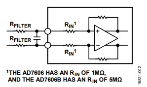
While the AD7606 has a 1 MΩ typical input impedance, the AD7606B has a 5 MΩ typical input impedance, making the AD7606B less sensitive to the gain error introduced by the input series resistance (RFILTER), as shown in Figure 2.


Bipolar Zero Code Error with RPD Resistor and No Sensor Connected
Traditionally, having a pull-down resistor (RPD) in parallel with the sensor (current transformer shown in Figure 3) allows users to detect when the sensor disconnects, that is if an ADC output code lower than 20 LSBs repeats for a number of samples (N).

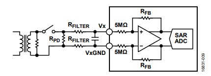
It is recommended to have an RPD much larger than the source impedance of the sensor to minimize the error that this parallel resistor may introduce. However, the larger the RPD, the larger the ADC output code generated when the sensor disconnects, which is not desired because a large ADC output code leads to unnoticed sensor disconnection. Because the AD7606B has larger RIN than the AD7606, for a given RPD, the ADC output code is lower if the sensor disconnects. For example, for a given RPD = 10 kΩ, the ADC output code is approximately 58 LSBs (±10 V range) on the AD7606 and approximately 11 LSBs on the AD7606B.


Throughput Rate
The AD7606B can sample as fast as 800 kSPS, whereas the maximum throughput rate for the AD7606 is 200 kSPS.
Temperature Range
The operating temperature range for the AD7606 is −40°C to +85°C, whereas the operating temperature range for the AD7606B is extended from −40°C to +125°C. All specifications stand across the whole temperature range, unless otherwise noted on the AD7606 or the AD7606B data sheet.
Software Mode
When the software mode of the AD7606B is enabled (see the Migrating to the AD7606B Using Software Mode section) rather than the legacy hardware mode, the following advanced features are available:
- Independent, per channel basis range selection, including a ±2.5 V range option.
- System gain, phase, and offset on-chip compensation.
- Sensor disconnect detection.
- Additional oversampling ratios (OSR): 128 and 256.
- Optional 1, 2, or 4 serial data output configurations.
- Diagnostics.
These features are only available within the software mode of the AD7606B, which can be configured by writing to the register map.
| Parameter | AD7606 | AD7606B | |
| Hardware Mode | Software Mode | ||
| Typical Input Impedance | 1 MΩ | 5 MΩ | 5 MΩ |
| Maximum Throughput Rate | 200 kSPS | 800 kSPS | 800 kSPS |
| Temperature Range | −40°C to +85°C | −40°C to +125°C | −40°C to +125°C |
| VDRIVE Range | 2.3 V to 5.25 V | 1.71 V to 3.6 V | 1.71 V to 3.6 V |
| Absolute Maximum Input Voltage | ±16.5 V | ±21 V | ±21 V |
| Analog Input Range | ±10 V or ±5 V1 | ±10 V or ±5 V1 | ±10 V, ±5 V, or ±2.5 V2 |
| System Gain, Phase, and Offset On-Chip Compensation | Not applicable | Not accessible | Available2 |
| Oversampling Ratio (OS) | From no OS to OSR = 64 | From no OS to OSR = 64 | From no OS to OSR = 256 |
| Sensor Disconnect Detection | Not applicable | Not accessible | Available2 |
| Serial Data Output Lines | 2 | 2 | Selectable: 1, 2 or 4 |
| Diagnostics | Not applicable | Not accessible | Available |
| 1 Not on a per channel basis. 2 On a per channel basis. |
|||
Migrating to the New Generation AD7606B
Migrating from the AD7606 to the AD7606B offers multiple advantages. All features available in the AD7606 are also available in the AD7606B. There is no need to change the layout or evaluation setup when migrating to the new generation of the product (AD7606B), as long as the digital supply is below 3.3 V and the parallel byte interface is not used.
Migrating to the AD7606B Using Hardware Mode
Using the Parallel Interface
To migrate to the AD7606B in hardware mode using the parallel interface, ensure that the following are done:
- Avoid tying the OS2, OS1, and OS0 pins high because the AD7606B enters software mode if this is done (as shown in Table 6). Note that this combination of the OS x pins is also invalid on the AD7606.
- Tie the PAR/SER SEL pin to AGND to select the parallel interface.
- After power-up, 253 µs (tDEVICE_SETUP) must elapse before initiating the first conversion. See Reset section for details on initiating subsequent resets.
Using Serial Interface
To migrate to the AD7606B in hardware mode using the serial interface, ensure that the following are done:
- Avoid tying OS2, OS1, and OS0 high simultaneously because the AD7606B enters software mode if this is done (as shown in Table 6). Note that the combination of the OS x pins is also invalid on the AD7606.
- Tie the PAR/SER SEL pin to VDRIVE to select the serial interface.
- Tie unused DBx pins to AGND.
- After power-up, 253 µs (tDEVICE_SETUP) must elapse before initiating the first conversion. See Reset section for details on initiating subsequent resets.
Note that the OS x/OSx pins are latched on the falling edge of RESET.
| OS 2 (OS2) to OS 0 (OS0) | AD7606 | AD7606B |
| 000 | No OS x | No OSx |
| 001 | 2 | 2 |
| 010 | 4 | 4 |
| 011 | 8 | 8 |
| 100 | 16 | 16 |
| 101 | 32 | 32 |
| 110 | 64 | 64 |
| 111 | Invalid | Enters software mode |
Migrating to the AD7606B Using Software Mode
To migrate to the AD7606B and take advantage of the advanced features only available in software mode, ensure that the following are done:
- Tie all of the OS x pins high to access software mode. The oversampling ratio is set through the corresponding register instead of through the pins.
- To access the AD7606B memory map using the serial interface, use Pin 29 (DB11/SDI) as the serial data input of the SPI interface. If Pin 29 is tied to AGND as recommended in the AD7606, no memory map write or read operation can be performed.
- To access the AD7606B memory map using the parallel interface, use Pin 10 (WR) for write operations. In the AD7606, Pin 10 (CONVST B) initiates conversions on Channel 5 to Channel 8. Tying Pin 10 of the AD7606 to CONVST A results in all eight channels sampling simultaneously. In the AD7606B, the WR pin must be available for the memory map to be accessed. If Pin 10 (WR) of the AD7606B is tied to Pin 9 (CONVST), a memory map write or read operation cannot be performed.
Software Compatibilty
The microcontroller code and its protocol, developed for the AD7606 products work with the AD7606B without requiring any modifications to be made as long as the device is used in hardware mode and the timing differences stated in the Reset section are respected. To take advantage of the features available in software mode, adapt the code to add writing capabilities to access the memory map in either the serial interface or the parallel interface (see the Migrating to the AD7606B Using Hardware Mode section and the Migrating to the AD7606B Using Software Mode section for additional information).
Author
