AN-1159: I²C-Compatible Interface on Cortex-M3 Based Precision Analog Microcontroller (ADuCxxx Family)
Introduction
This application note describes the hardware master and slave implementation of an I2C-compatible (inter-integrated circuit) interface using the Cortex-M3 based family of precision Analog Devices, Inc., microcontrollers (the ADuCxxx family).
This application note also includes example code showing how a master and a slave can communicate with each other using the I2C interface. These examples are:
- Master transmit and receive
- Slave transmit and receive
- DMA transfers (transmit and receive) in slave mode
- DMA transfers (transmit and receive) in master mode
See the AN-1159 companion code zip file, available on https://www.analog.com for companion codes.
The main features of the I2C bus are:
- Only two bus lines are required, a serial data line (SDA) and a serial clock line (SCL). Both of these lines are bidirectional, meaning that both the master and the slave can operate as transmitters or as receivers.
- An I2C master can communicate with multiple slave devices. Because each slave device has a unique address, single master/slave relationships can exist at all times even in a multi-slave environment.
- Arbitration features allow multiple masters on the same I2C bus.
- The master and slave can transmit and receive at up to 400 kbps.
- On-chip filtering rejects <50 ns spikes on the SDA and the SCL lines to preserve data integrity. Figure 1 shows typical I2C connections for multiple devices.


I2C Fundamentals
I2C Interface Overview
I2C is a 2-wire serial communication system originally developed by Philips Semiconductors (now NXP Semiconductors) that allows multiple masters and multiple slaves to be connected via two wires (SCL and SDA). In an I2C interface, there must be at least a single master and a single slave.
The SCL signal controls the data transfer between master and slave. One clock pulse must be generated for each data bit transferred. The SCL signal is always transmitted from the master to the slave. The slave, however, does have the ability to pull this line low if it is not ready for the next transmission to begin. This is called clock stretching.
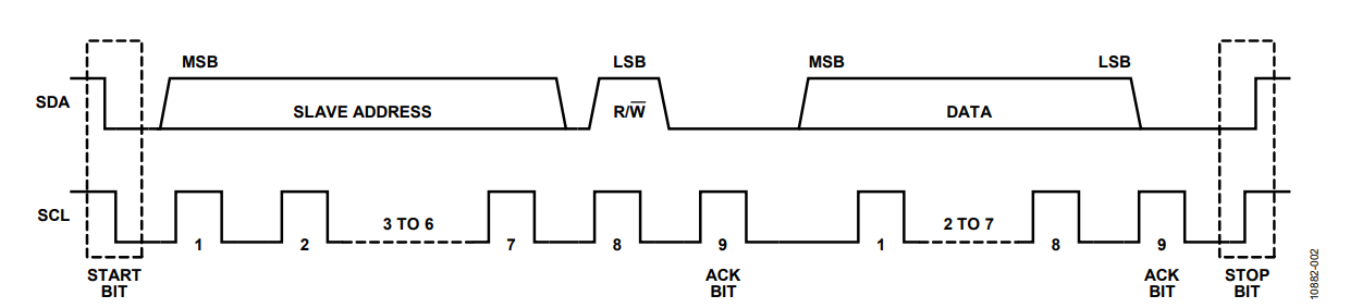
The SDA signal is used to transmit or receive data. The SDA input must be stable during the high period of SCL. A transition of the SDA line while SCL is high is seen as a start or stop condition. A typical transfer sequence is shown in Figure 2.

Start Condition
A typical data transfer sequence for an I2C interface starts with the start condition. The start condition is simply a high to low transition in the SDA line while the SCL line is pulled high (see Figure 3). The master is always responsible for generating the start condition. The start (and stop) conditions are the only times that the SDA line should change during a high period of the SCL line. During normal data transfer (including slave addressing), the data on the SDA line must be stable during the high period of the SCL line.


Stop Condition
The data transfer sequence is terminated by the stop condition. A stop condition is defined by a low-to-high transition on the SDA line while SCL is high (see Figure 4).

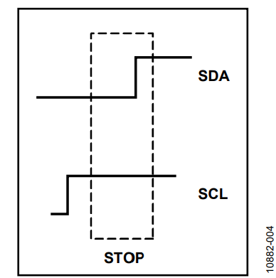
The stop condition is always generated by the master. The master sends the stop condition once the master is satisfied that the data sequence is over or if it receives a NACK from the slave device. The reception of the stop condition resets the slave device into waiting for the slave address again.
The I2C interface can be configured to generate an interrupt on the stop condition.
Slave Address
After the start condition, the master sends a byte, most significant bit (MSB) first, on the SDA line, along with eight SCL pulses. The first seven bits of this byte is the 7-bit slave address. The slave only responds to the master if this 7-bit address matches the address of the slave device (or one of the four slave addresses). The eighth bit, the least significant bit (LSB), is the R/W status bit. The R/W status bit determines the direction of the message. If this bit is low, the master writes data to a selected slave. If this bit is set, the master expects to receive data from the slave. The master generates the clock in both cases.
If the slave receives the correct address, that is, the seven MSBs from the master match the seven MSBs of the I2CADR0 memory mapped register (MMR), the slave returns a valid ACK, pulls the SCL line low, and sets flags in the I2CSSTA.
While the slave does all the manipulation of the I2C slave addressing automatically in hardware, it is up to the master to output the slave address appropriately.
Acknowledge (ACK)/No Acknowledge (NACK)
If the slave address matches the address sent by the master, the slave automatically sends an acknowledge (ACK). Otherwise, it sends a no acknowledge (NACK). An ACK is seen as a low level on the SDA line on the ninth clock pulse. A NACK is seen as a high level on the SDA line on the ninth clock pulse (see Figure 5).


During data transfer, the ACK or the NACK is always generated by the receiver. Note, however, that the clock pulse required for the ACK is always generated by the master. The transmitter must release the SDA line (high) during the ACK clock pulse. For a valid ACK, the receiver must pull the SDA line low.
Both the ACK and the NACK are automatically generated in hardware, at the end of each byte in the reception.
If a master receives a NACK from a slave-receiver (either the slave did not respond to the slave address or the data transmitted), the master should generate the stop condition to abort the transfer (see the Data Transfer section).
A master receiver must signal the end of a data sequence to the slave-transmitter by generating a no acknowledge (NACK) after the last byte that was sent by the slave. Once the slave receives the NACK, it releases the SDA line to allow the master to generate the stop condition.
The slave can also be configured to force a NACK.
Data Transfer
In the I2C interrupt service routine (ISR), or in a polled implementation, the slave decides whether to transmit or receive depending on the status of the R/W bit sent by the master. The slave then either transmits or receives a bit on each clock sent by the master. It is up to the master to provide the nine clocks (eight for the data and one for the ACK) for the slave to transmit/receive data to/from the master. The I2C interrupt bit is set every time a valid data byte is transmitted or received by the slave.
Note again that in a slave-transmitter, master-receiver system the master must signal the end of a data sequence to the slave by sending a NACK after the last byte transmitted by the slave. Once the slave receives the NACK, it releases the SDA line to allow the master to generate the stop condition.
If a master wants to abort a data transfer or to interrupt the data transfer of another master on the bus, it can do this by sending a start condition followed by a stop condition.
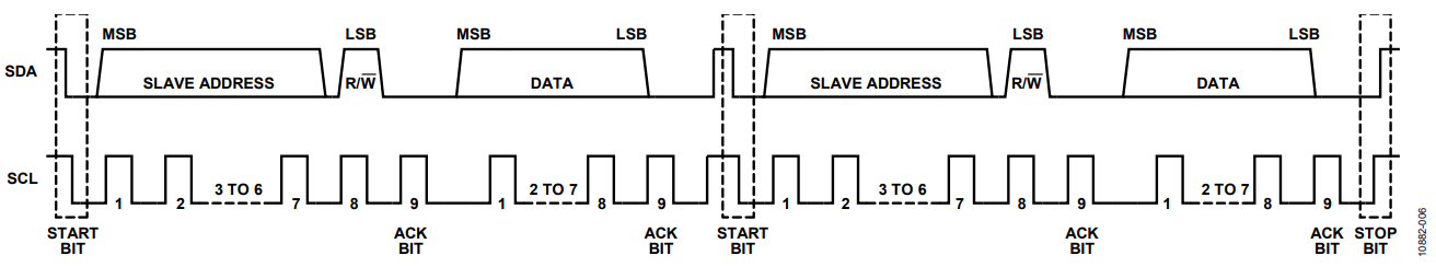
Repeated Start Condition
A repeated start condition occurs when a second start condition is sent to a slave without a stop condition being sent in between. This allows the master to reverse the direction of the transfer, by changing the R/W bit without having to give up control of the bus.
An example of a transfer sequence is shown in Figure 6. This is generally used where the first data sent to the part sets up the register address to be read from. An interrupt is generated when a “repeated start + slave address” is received. This can be differentiated from a “start + slave address” by using the status bits in the I2CxSSTA MMR.
The ADuCxxx family can directly generate an I2C repeated start sequence when in master mode using the sequence shown in Figure 6.

Clock Stretching
In an I2C communication, the master device determines the clock speed. Unlike RS-232, the I2C bus provides an explicit clock signal that relieves master and slave from synchronizing exactly to a predefined baud rate.
However, there are situations where an I2C slave is not able to cooperate with the clock speed given by the master and needs to slow down a little. This is done by a mechanism referred to as clock stretching.
An I2C slave is allowed to hold down the clock if it needs to reduce the bus speed. The master, on the other hand, is required to read back the clock signal after releasing it to a high state and wait until the line has actually gone high.
    I2cFifoFlush(MASTER, ENABLE);
    I2cFifoFlush(MASTER, DISABLE);
    NVIC_DisableIRQ(I2CM_IRQn);
    I2cMWrCfg(0xA0); // configure to send slave address
    I2cTx(MASTER, ucStartAddress); // send slave address
    while ((I2cSta(MASTER)& I2CMSTA_TXFSTA_EMPTY) != I2CMSTA_TXFSTA_EMPTY){} {}
    // wait for the Tx FIFO to empty
    I2cMRdCfg(0xA0, ucLength , DISABLE);
    // sends out the read condition, this function sets the read bit
    NVIC_EnableIRQ(I2CM_IRQn);
Typical I2C Timing Diagrams
Table 1 and Table 2 give the typical timing on the I2C bus implemented on the Cortex-M3–based precision analog microconverters. The capacitive load for each of the I2C-bus line, Cb, is 400 pF maximum as per I2C-bus specifications.
Note that the internal pull up on SCL and SDA should be disabled in software.
| Parameter | Description | Min | Max | Unit |
| tL | Clock low pulse width | 1300 | ns | |
| tH | Clock high pulse width | 600 | ns | |
| tSHD | Start condition hold time | 600 | ns | |
| tDSU | Data setup time | 100 | ns | |
| tDHD | Data hold time | 0 | ns | |
| tRSU | Setup time for repeated start | 600 | ns | |
| tPSU | Stop condition setup time | 600 | ns | |
| tBUF | Bus-free time between a stop condition and a start condition | 1.3 | μs | |
| tR | Rise time for both clock and data | 20 + 0.1 Cb | 300 | ns |
| tF | Fall time for both clock and data | 20 + 0.1 Cb | 300 | ns |
| tSUP | Pulse width of spike suppressed | 0 | 50 | ns |
| Parameter | Description | Min | Max | Unit |
| tL | Clock low pulse width | 4.7 | µs | |
| tH | Clock high pulse width | 4.0 | µs | |
| tSHD | Start condition hold time | 4.7 | µs | |
| tDSU | Data setup time | 250 | ns | |
| tDHD | Data hold time | 0 | µs | |
| tRSU | Setup time for repeated start | 4.0 | µs | |
| tPSU | Stop condition setup time | 4.0 | μs | |
| tBUF | Bus-free time between a stop condition and a start condition | 4.7 | µs | |
| tR | Rise time for both clock and data | 1 | µs | |
| tF | Fall time for both clock and data | 300 | ns |


I2C Implementation on the Cortex–M3–based Microconverter
The Cortex-M3–based ADuCxxx family contains full hardware master and slave I2C ports.
The I2C peripheral interface consists of 19 registers in total, 9 for the master, 9 for the slave and one shared between master and slave. These are summarised in Table 3.
| Registers | Master | Slave | Shared |
| Receive | I2CMRX | I2CSRX | I2CFSTA |
| Transmit | I2CMTX | I2CSTX | I2CFSTA |
| Status | I2CMSTA | I2CSSTA | |
| Control | I2CMCON | I2CSCON | |
| Address/ID | I2CADR0/ I2CADR1 |
I2CID0/I2CID1/ I2CID2/I2CID3 |
|
| Clock | I2CDIV | ||
| Other | I2CMRXCNT/ I2XMCRXCNT |
I2CALT |
All registers and bits are described in the device user guide.
Some specific features are explained in more details in this application note.
Configuring The Communication Speed
The I2CDIV is a 16-bit register containing two 8-bit values, HIGH and LOW. The value in this register sets up the speed of the I2C bus. This is set up according to the formula:
fI2CSCL = fPERIPH/(LOW + HIGH + 3)
where:
fPERIPH = is the I2C peripheral clock
HIGH = I2CDIV[15:8]. The high period of the I22C bus clock is determined by (HIGH + 2) ÷ I2C peripheral clock. LOW = I2CDIV[7:0]. The low period of the I2C bus clock. is determined by (LOW + 1) ÷ I2C peripheral clock.
Thus, for 100 kHz operation, with an I2C peripheral clock of 16 MHz, LOW = 0x4F, and HIGH = 0x4E and for 400 kHz, LOW = 0x13, and HIGH = 0x12.
ADuCM360 Specific
On the ADuCM360, the I2C peripheral clock is:
fPERIPH = fUCLK÷ (CLKSYSDIV × I2CCLK)
where:
UCLK is the system clock, 16 MHz. CLKSYSDIV is 1 or 2, depending on the CLKSYSDIV[0] bit setting.
I2CCD is the clock divide value and is set by the CLKCON1[8:6] bits to value between 1 and 7.
The I2C peripheral clock is disabled by default and should be first enabled in CLKDIS[2]. This is for optimizing power consumption on the part. For more details, see the AN-1111 Application Note, Options for Minimizing Power Consumption When Using the ADuCM360/ADuCM361.
The following flowcharts assume that the I2C peripheral clock is enabled and configured.
Use of the FIFO
The I2C hardware interface includes four 2-byte FIFOs per I2C function.
- Master receive
- Master transmit
- Slave receive
- Slave transmit
Each of them also includes a shift register holding the remaining bit of a byte to receive/transmit.
Transmit FIFO
To transmit data, the I2CSTX/I2CMTX registers must be loaded.


Writing a byte to the Tx register is equivalent to writing to Byte 1 of the FIFO (see Figure 8).
- If Byte 0 is empty, the byte in Byte 1 gets pushed to Byte 0 automatically. This is transparent to the user. I2CFSTA register indicates when one byte is present in the FIFO.
- If Byte 0 is already full, the byte stays in Byte 1. Writing in Tx again overwrites Byte 1.
The transition of Byte0 to the shift register (OUT) is also transparent to the user but requires a valid communication on the slave side.
The FIFO set the TXREQ bit (I2CMSTA[2]/I2CSSTA[2]) when it is not full. These bits can generate interrupts if enabled.
Setting the transmit FIFO flush bit(s) in the I2CFSTA register empties the FIFO(s).
Receive FIFO
When receiving data, the data arrives in Byte 0.
- If Byte 1 is empty, Byte 0 is shifted automatically to Byte 1.
- If Byte 1 is already full, Byte 0 stays until I2CSRX is read (equivalent to reading Byte 1).
- If other data arrive while the FIFO is full, the slave delivers a NACK for the data and I2CSSTA[4] is set. (or I2CMSTA[9] for the master)
The FIFO set the RXREQ bit (I2CMSTA[3]/I2CSSTA[3]) when it is not empty. These bits can generate interrupts if enabled.


Use of the DMA Channels
Four channels in the DMA controller are allocated to the I2C interface:
- Master receive
- Master transmit
- Slave receive
- Slave transmit
When transmitting, the I2C peripheral generates a DMA request when there is space in the transmit FIFO and when receiving, when there is a byte in the receive FIFO.
The DMA transfer ends, and generates an interrupt, when all bytes from memory have moved to the transmit FIFO or when the memory allocated to the DMA channel is full.
The I2C status bits TXREQ and RXREQ do not generate interrupts when set in DMA mode; however, the TCOMP bit indicating the end of the transaction can still generate an interrupt and be used in DMA mode.
I2C Low Level Functions
To simplify code development, a set of low level functions are provided in I2cLib. These functions are listed in Table 4. They are described in detail in the documentation folder of the CD/DVD.
The flowcharts for each scenario are based on these low level functions.
| Master Configuration | Description |
| int I2cMCfg(int iDMACfg, int iIntSources, int iConfig); | Configure I2C master |
| int I2cBaud(int iHighPeriod, int iLowPeriod); | Configures I2C baud rate |
| int I2cMWrCfg(unsigned int uiDevAddr); | Configures slave address |
| int I2cMRdCfg(unsigned int uiDevAddr, int iNumBytes, int iExt); | Configures slave address, number of bytes to read |
| int I2cMRdCnt(void); | Read the counter of bytes received by the master |
| Slave Configuration | Description |
| int I2cSCfg(int iDMACfg, int iIntSources, int iConfig); | Configures I2C slave |
| int I2cSIDCfg(int iSlaveID0, int iSlaveID1, int iSlaveID2, int iSlaveID3); | Configure the slave addresses |
| int I2cSGCallCfg(int iHWGCallAddr); | Setup the hardware general call |
| Common Functions | Description |
| int I2cRx(int iMode); | Reads the Rx register of the slave or master |
| int I2cTx(int iMode, int iTx); | Writes in the Tx register of the slave or master |
| int I2cStr(int iMode, int iStretch); | Configures clock stretching |
| int I2cFifoFlush(int iMode, int iFlush); | Flush slave or master Tx FIFO |
| int I2cSta(int iMode); | Reads the status of the slave or master |
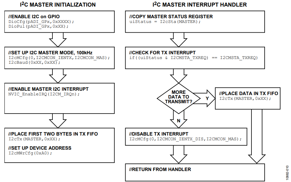
Master Transmit
In order to transmit a byte, the data must first be loaded into the transmit FIFO. The address of the slave must be specified in the I2CADR0 register. For a write of data, the write (W) bit in the address register must be set to zero. Writing to the I2CADR0 register automatically generates a start condition.
An I2C interrupt is generated on the first clock of a byte transmitted, when the transmit FIFO is empty or not full, and Bit 2 in I2CMSTA is set, indicating that the master has just transmitted a byte. This allows the user to add a byte to the FIFO. The status of the FIFO can be check in I2CMSTA[1:0] or the I2CFSTA register.
If only one byte is in the FIFO when initiating the transfer, the first I2C interrupt occurs on the first clock of the address transmitted. If two bytes are in the FIFO, then the interrupt is generated on the first clock of the first byte transmitted.
If the transmit FIFO is not kept full, the transmit interrupt is generated on each clock edges. The TXUR bit is then set after the last bit of the last byte has been transmitted. If no data is placed in the FIFO within ½ clock cycle of the TXUR being set, that is, during the slave acknowledge bit, the master automatically ends the transmission.
The stop condition is automatically generated 5.1 µs after the last byte is transmitted.
The TXREQ interrupt enable bit in the I2CMCON MMR (I2CMCON[5]) needs to be cleared or the transmit interrupt will be generated continuously until the STOP condition is generated.
The TCOMP bit also generates an interrupt if enabled (I2CMCON[8]), when the stop condition is generated. This allows to safely turning off the I2C peripheral, for example before entering low power mode.
An example of the master responding to a request for data from the slave is shown in Figure 10.

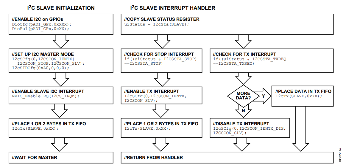
Slave Receive
As the data is received by an I2C slave, an interrupt is generated after the eighth clock of each byte is received. If the FIFO is not read before a third byte is received, RXOF, I2CSSTA[4] is set, indicating a receive FIFO overflow. The FIFO can be read at this time. If the FIFO is not read before the rising edge of the ninth clock, the slave interface automatically delivers a NACK.
To read data from the FIFO, the I2CRX register is used. RXREQ, I2CSSTA[3] indicates that the slave has received data.
Only reading I2CRX clears this bit. The I2C interrupt is generated continuously if enabled and RXREQ is set.
The master automatically sends a stop condition after sending the last data. The slave detects a STOP condition sets I2CSSTA[10]. This bit can generate an interrupt if IENSTOP, I2CSCON[8] is set.
A flowchart of the slave receiving bytes from the master is shown in Figure 11. Figure 12 shows when the status bits are set and when the interrupts occur.


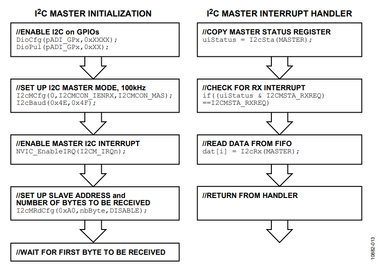
Master Receive
In master mode, to read data from a slave, a similar approach is used. First, the number of bytes to be read is configured by the I2CMRXCNT register. This denotes the number of bytes to be read from the slave, plus one. This is a 8-bit register so 256 bytes can be received at once. An EXTEND option is also available for larger transfer. The I2CMCRXCNT reflects the current number of bytes received by the master.
In order to start receiving data, the read (R) bit is set in the I2CADR0 register. This initiates a transfer with a start condition generated with the address and a R/W bit set by the I2CADR0 register. After each byte is received (after the ninth clock, ACK or NACK), an interrupt is generated. RXREQ, I2CMSTA[3] is set, indicating that a byte has just been received. Only reading I2CMRX clears this bit.
When the master does not need to receive more data, it automatically generates a NACK to the last byte received. This tells the slave to cease transmitting bytes and allows the master to then generate a stop condition.
If the data received is not read on time and the FIFO is full, the master delivers a NACK for the extra data received.
A flowchart of the master receiving bytes from the slave is shown in Figure 13.

Slave Transmit
The slave generates an interrupt on each request for data to be transmitted, the first occurring after the ACK of the address, that is, while Byte 0 of the FIFO is sent. Data needs to be preloaded into the slave transmit FIFO, otherwise the first read request from the master results in a NACK being generated. If the FIFO is preloaded with two sets of data, one interrupt occurs after the ACK of the address and then after the ACK of each byte sent. If the FIFO is preloaded with one set of data only, two interrupts occur after the ACK of the address, the FIFO emptying after sending the first data.
Once a byte has been transmitted, an interrupt is generated as long as the master continues to request data.
TXREQ, I2CSSTA[2] is set when there is space in the transmit FIFO, or each time a byte is transmitted to the master. The transmit interrupt can be disabled when there is no more data to transmit and can be re-enabled when detecting the STOP condition (I2CSSTA[10]). The STOP detection can generate an interrupt if IENSTOP, I2CSCON[8] is set.
An example of the slave responding to a request for data from the master is shown in Figure 14. Figure 15 shows when the status bits are set and when the interrupts occur.


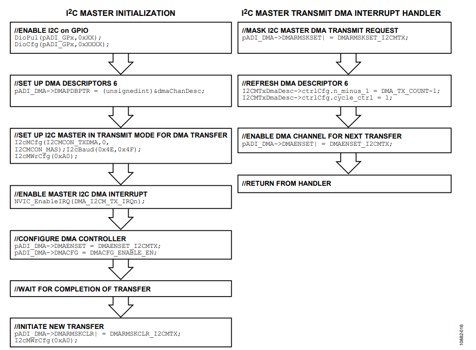
DMA Mode, Master Transmit
I2C transfers are initiated with the transmission by the master of the slave address. When DMA transmit mode is configured, by setting TXDMA in the I2CMCON MMR, the transfer starts when the I2C peripheral is fully configured, that is, baud rate, slave address, and DMA transmit request, and when the DMA controller is configured and enabled. The I2C master transmit DMA channel should also be enabled in the NVIC at any time before starting the transfer.
The DMA transfer is complete when all bytes have been transferred from memory into the FIFO; this means while the last two bytes are stored in the FIFO and the third last byte is being transmitted as shown in Figure 17. The DMA channel is then disabled automatically in the DMA controller. However, the I2C peripheral sends a DMA request to the DMA controller when the FIFO is not full and generates an interrupt. Therefore, the I2C requests should be masked in the DMA controller to avoid multiple interrupts (DMARMSKSET).
The DMA controller needs to be reconfigured/re-enabled to start a new transfer.
Figure 16 shows a flowchart of I2C master transmit DMA transfer.


DMA Mode, Master Receive
DMA transfers are enabled in the I2C peripheral by setting RXDMA in the I2CMCON MMR. The transfer starts when the DMA controller is configured and enabled and when I2C peripheral is fully configured, that is, baud rate, slave address, and DMA transmit request. The I2C master transmit DMA channel should also be enabled in the NVIC at any time before starting the transfer.
The DMA transfer is complete when all bytes expected by the DMA controller have been received. The I2CMRXCNT MMR should be also configured with the same number of bytes.
When the DMA transfer is complete, the corresponding channel is disabled automatically in the DMA controller. The DMA controller needs to be reconfigured and re-enabled to start a new transfer. Initiation of a new transfer is done by writing the slave address again in the I2CADR0 MMR.
Figure 18 shows a flowchart of DMA transfer with the master receiving data from the slave.


DMA Mode, Slave Receive and Transmit
DMA transfers are enabled in the I2C peripheral by setting TXDMA and/or RXDMA in the I2CSCON MMR. The I2C peripheral should be configured in slave mode and the I2C interrupt disabled. NVIC and DMA controller need to be configured. The DMA transfer is initiated by reception of the correct I2C address. Only the data bytes are then transferred into memory. When the DMA transfer is complete, the corresponding channel is disabled automatically in the DMA controller. Only the DMA controller needs to be reconfigured to start a new transfer. Figure 19 shows a flowchart of DMA transfer with the slave transmitting and receiving.
Note that the DMA transfer in transmit mode ends when the 3rd to last byte is being transmitted, similar to master transmit.

Companion Codes
A list and description of companion codes provided is shown in Table 5.
| Mode/Flowchart | Code Example/Tools |
| Master Transmit | I2Cmaster.c |
| Slave Receive | 2Cslave.c |
| Master Receive | I2Cmaster.c |
| Slave Transmit | I2Cslave.c |
| DMA Mode, Master Transmit | I2CmasterDMA.c |
| DMA Mode, Master Receive | I2CmasterDMA.c |
| DMA Mode, Slave Receive and Transmit | I2CslaveDMA.c |
Author
