

运算放大器
子分类
分类产品
相关资源






相关工具
通过 LTSPICE 仿真演示来介绍放大器指标,告诉大家这个指标会对电路产生什么影响。
LTpowerCAD®程序是一款完整的电源设计工具,可显著简化电源设计任务。它专门针对采用凌力尔特(现为ADI公司的一部分)电源产品的用户应用提供元件值和性能估算值建议。在LTpowerCAD程序中,还有一个用于系统级电源设计和优化的LTpowerPlanner电源架构设计工具。
使用光电二极管向导设计跨导放大器电路与光电二极管接口。从工具内置器件库中选择一个光电二极管,或输入自定义光电二极管规格。快速考量权衡带宽、峰值(Q)和ENOB/SNR。修改电路参数,并立即查看图中的脉冲响应、频率响应和噪声增益结果。
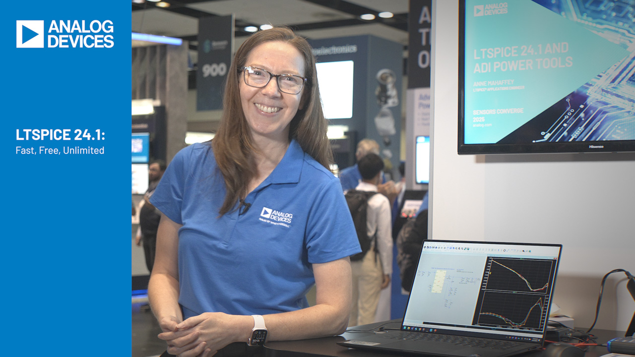
LTspice®是一款高性能SPICE仿真软件、原理图采集和波形查看器,集成增强功能和模型,简化了模拟电路的仿真。宏模型也包括在LTspice下载中,适用于大多数ADI开关稳压器、放大器以及用于通用电路仿真的器件库。
LTspice®是一款高性能SPICE仿真软件、原理图采集和波形查看器,集成增强功能和模型,简化了模拟电路的仿真。宏模型也包括在LTspice下载中,适用于大多数ADI开关稳压器、放大器以及用于通用电路仿真的器件库。


FAQs
What are Operational Amplifiers (Op Amps)?
Operational amplifiers (op amps) are high-gain voltage amplifiers with differential inputs and a single output. They serve as fundamental building blocks for amplification, filtering, signal conditioning, integration, and differentiation. Available in precision, high-speed, and power variants, op amps are essential in sensor interfaces, data acquisition systems, and analog control loops.
How do I design a basic inverting amplifier using an op amp?
To design a basic inverting amplifier, connect the input signal through resistor Rin to the inverting input, with feedback resistor Rf from output to that node; gain is −Rf/Rin. Ground the non-inverting input only for suitable dual supplies or ground-centered signals. On single supplies, use a reference voltage. Check headroom, resistor noise, bias-current error, bandwidth, stability, load drive, and decoupling.
How does an op amp function as an integrator in electronic circuits?
An op amp integrator uses input resistor R and feedback capacitor C, ideally giving VOUT = −(1/RC)∫VIN dt. A parallel resistor limits DC gain and sets the low-frequency cutoff. Check initial conditions, output headroom, offset, and bias-current errors. For a practical implementation, see EVAL-KW4101Z and verify the amplifier’s operating limits.
Can you recommend ways to improve the slew rate of an op amp?
To improve op amp slew rate, select a device with a higher slew rate specification suited to your signal frequency and amplitude requirements. Reduce output voltage swing and minimize load capacitance. Check large-signal bandwidth, output-current demand, compensation, minimum stable gain, and stability. Avoiding unity-gain configurations does not inherently improve slew rate, and external circuitry cannot increase the intrinsic slew rate.
Are there any step-by-step guides for troubleshooting op amp circuits?
When troubleshooting op amp circuits, verify power supply voltages and decoupling capacitor placement. Use an oscilloscope to check for output oscillations. First consult the datasheet for operating limits, then check pinout, enable state, grounding, feedback, output load, saturation recovery, capacitive loading, soldering, layout, and probing. Use product-specific notes; Analog Filter Wizard is a filter-design tool, not a general diagnostic guide.

{{modalTitle}}

{{modalDescription}}
{{dropdownTitle}}

- {{defaultSelectedText}} {{#each projectNames}}
- {{name}} {{/each}} {{#if newProjectText}}
-
 {{newProjectText}}
{{/if}}
{{newProjectTitle}}

{{projectNameErrorText}}