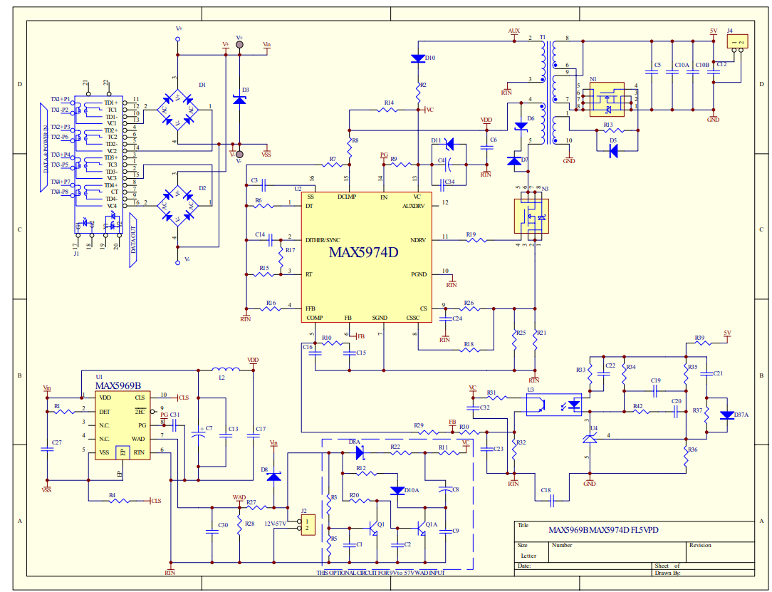
This reference design is for a highly efficient, flyback, 5V Class 3 powered device (PD) with a wide 9V to 57V auxiliary input. The design features the MAX5969B as its controller. The design also uses the MAX5974D, which controls current-mode PWM converters and provides frequency foldback for both the auxiliary input and power over Ethernet (PoE) applications. Using these devices, this reference design is IEEE® 802.3af/at compliant. It is also a high-performance, compact, and cost efficient solution for a Class 3 PD. The design can also support the wide auxiliary-input voltage range to provide 10W output power.
General Description
This reference design features the MAX5969Band MAX5974D. The MAX5969B controller is fully compliant with the IEEE 802.3af/at standard in a power-over-Ethernet (PoE) system. The device can also be powered from a wall adapter (WAD). The MAX5974D controls wide 9V to 57V input-voltage, active-clamped, current-mode PWM converters and provides frequency foldback. Using these devices, this reference design is IEEE 802.3af/at compliant. It is also a high-performance, compact, and costeffective solution for a Class 2 PD or a Class 3 PD.
Specifications:
- The 5V/2.6A PD meets the following specifications:
- Input voltage: 36V to 57V
- WAD input voltage: 9V up to 57V
- VOUT: 5V/2.6A
- Output ripples: ±2%
- Load transient VP-P: ±2% (50% step-load)
- Line and load regulation: ±0.2%
- Total efficiency with a load of 2.5A at 5V and a 48V input: 87.4% (not including input LAN transformer and diode bridge)

Top view of the reference design

Bottom view of the reference design


Transient Response
- VIN = 40V, IOUT2 = 1A–2.5A
- Ch1: 100mV/div, 5V output voltage
- Ch4: 1A/div, output current
- Time base: 2ms/div

Transient Response
- VIN = 16V, IOUT2 = 1A–2.5A
- Ch2: 200mV/div, 5V output voltage
- Ch4: 1A/div, output current
- Time base: 2ms/div


