Interfacing Linduino to LTC2508-32
Introduction
LTC2508-32 is a fast, 32-bit SAR ADC with an integrated configurable digital averaging filter. The demo board, DC2222A-B, has connectors to talk to DC890, as well as Linduino. The demo manual describes how to connect the board to a DC890 and to run PScope. It also explains how to use a Linduino (or a DC590B board) to run QuikEval and read data at a very slow data rate. But what if you want your Linduino to go faster?
This blog aims at showing how to have high speed data capture from LTC2508-32 using a Linduino. The QuikEval connector on the Linduino does not have enough GPIO lines to control the Down-sampling Factor (DF) selection pins (SEL1, SEL0) of the filter. Hence, the on-board FPGA controls the SEL lines after receiving the initial configuration data. An I/O expander (that our engineers call a “Sneaker Port”) is used to send configuration information to the on-board FPGA through SPI, which in turn, sets the SEL lines. If this is confusing, keep reading and it will start making sense.
Linduino is not fast enough to capture data from LTC2508 at its full sampling speed. However, with highly optimized code, avoiding timeouts using interrupts and gearing up the SPI clock to 4 MHz, you can achieve a reasonable amount of sampling speed. This is explained in the last section of this blog.
Details of the Part
The LTC2508-32 features two digital serial interfaces, one with the filtered output data and the other with no-latency output data. The QuikEval connector on Linduino is connected to the filtered output serial interface (SDOA).
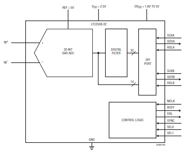
Figure 1. Block diagram of LTC2508
The filtered output is updated only once every DF number of conversions after a SYNC pulse. Each rising edge on the MCLK pin initiates a new conversion. Hence, the filtered output is available in the I/O register after DF number of MCLK pulses. Refer to the flow chart below or read more about this in the LTC2508-32 datasheet. The digital filter can be easily configured for four different down-sampling factors by pin strapping SEL0 and SEL1.
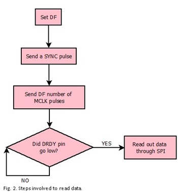
Details of the Demo Board
This section aims to explain how the on board FPGA sets the SEL pins based on the configuration data sent to it. The FPGA waits for the configuration data which is a sequence of 16 bits, sent through SPI. The 16 bits of configuration data to be sent to FPGA are:
| 15 | 14 | 13 | 12 | 11 | 10 | 9 | 8 | 7 | 6 | 5 | 4 | 3 | 2 | 1 | 0 |
| 1 | 0 | 0 | 0 | 0 | SEL0 | SEL1 | 0 | 0 | 0 | 0 | 0 | 0 | 0 | 0 | 0 |
Bit 15: Select serial interface. 1 = SDOA, 0 = SDOB
Bit 10: SEL0
Bit 9: SEL1
Rest of the bits are used by other parts in the LTC25XX family.
| SEL1 | SEL0 | DF |
| 0 | 0 | 256 |
| 0 | 1 | 1024 |
| 1 | 0 | 4096 |
| 1 | 1 | 16384 |
The SPI lines of the FPGA are tied to P5, P6 and P7 of the Sneaker Port (CS_IN, SDI_IN and SCK_IN), as shown in the figure below. These pins are bit banged to create a SPI port to the FPGA. Bit banging of P0-P7 of the Sneaker Port is done by transmitting I2C data from the Linduino to the Sneaker Port, and this is explained in the section below.
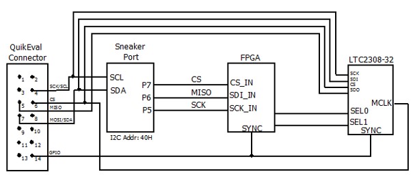
Figure 3. Connection Diagram for the entire system
Communication to “Sneaker Port”

Bit banging of the output pins of the Sneaker Port is done by sending I2C data. To talk I2C to the Sneaker Port, the first byte is the I2C address of the chip, and the second byte is the data to P0-P7. The SPI pins to the FPGA are CS = P7, SDI = P6, and SCK = P5. The state of each of the P0-P7 pins translates into a unique I2C byte.
| SPI State | P7 | P6 | P5 | P4 | P3 | P2 | P1 | P0 | I2C Byte |
| CS low, SDI low, SCK low | 0 | 0 | 0 | 0 | 0 | 0 | 0 | 0 | 0 |
| CS low, SDI low, SCK high | 0 | 0 | 1 | 0 | 0 | 0 | 0 | 0 | 0×20 |
| CS low, SDI high, SCK low | 0 | 1 | 0 | 0 | 0 | 0 | 0 | 0 | 0×40 |
| CS low, SDI high, SCK high | 0 | 1 | 1 | 0 | 0 | 0 | 0 | 0 | 0×60 |
Note:
To transmit a 0 on the SDI line, we need to hold the data line low and have the SCK line go low, high and low. This is achieved by transmitting 0×00, 0×20 and 0×00.
Note:
To transmit a 1 on the SDI line, we need to hold the data line high and have the SCK line go low, high and low. This is achieved by transmitting 0×40, 0×60 and 0×40.
Note:
If the user would like to use their own board to interface to the DC2222A, it is necessary to drive pin 2 of the QuikEval Connector to VCCIO, so that the FPGA of the DC2222A knows there is a controller connected and will listen for its commands.
Linduino Code:
LTC2508 talks SPI and those signals are separately accessed through the QuikEval connector to read data out of the part. You can find the Linduino code here.
Linduino code can be explained in three separate sections:
a) Function: void sneaker_port_init()
This function writes the configuration data to then FPGA and then, sends a SYNC pulse.
// P3 = 0 pulls WRIN_CS low
i2c_write_byte(SNEAKER_PORT_ADDRESS, CS_LOW);
for(i = 0; i < 48; ++i)
{
// Sending configuration data
i2c_write_byte(SNEAKER_PORT_ADDRESS, i2c_data[i]);
}
// P3 = 1 pulls WRIN_CS high
i2c_write_byte(SNEAKER_PORT_ADDRESS, CS_HIGH);
b) Function: void send_pulses (uint8_t pin, uint16_t num_of_pulses)
This function sends DF number of pulses to the CS pin which is connected to the MCLK of LTC2508.
c) Function: uint32_t LTC2508_read_data(uint8_t QUIKEVAL_CS, uint16_t *DF)
Read data out of LTC2508-32 through regular SPI using connections on the QuikEval connector.
Optimizing the project
As mentioned before, Linduino is not fast enough to have high speed data acquisition from LTC2508. However, with the following steps, we can have a reasonable rate of reading out data. This modified Linduino code can be found at:
LTSketchbook\Part Number\2000\2500\2508\DC2222_interrupt_driven_read
- MCLK is driven by an external clock source to avoid delay in toggling the CS pin.
- DRDY is connected to INT1. An interrupt is triggered when the Data Ready (DRDY) pin goes low, ie., when the data is ready after a conversion; at which time, it is read out.
- In the Linduino code, data is continuously captured in the interrupt service routine and printed out to the serial console as hex values. Converting the data to voltage can be done later.
- The serially printed out data is logged into a file using TeraTerm. Setting up Tera Term is explained in the following sections.
- The data is read out, converted to voltage and plotted using a Python script.
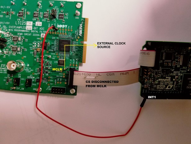
Figure 5. LTC2508 DRDY# connected to INT1 (digital pin 3)
Figure 6 is a scope shot showing the data on SDOA line after a pulse on the DRDY pin. DRDY pin triggers after DF number of pulses on MCLK.
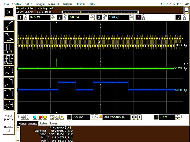
Figure 6. Scope shot showing data on SDOA after DRDY pulse.
With an MCLK of 100 kHz and DF = 256, the data rate achievable is 390.635 Hz, as shown in the scope shot below.
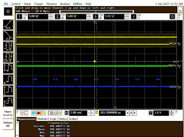
Figure 7. Continuous DRDY pulses and data following on the SDOA line.
How to set TeraTerm:
- Install Tera term using this link.
- Open Tera Term.
- If the New Connection tab has not opened up already, go to File à New Connection.
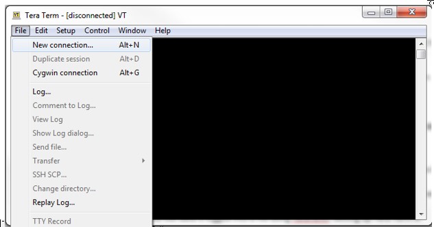
Figure 8. Setting up new connection on Tera Term.
- Make sure the Linduino USB is plugged in.
- Select Serial connection and the correct Serial port.
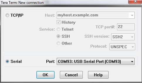
Figure 9. Setting up Serial COM port.
- Go to Setup à Serial Port.
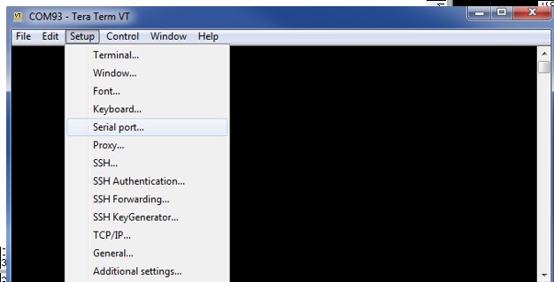
Figure 10. Opening Serial port.
- Set Baud Rate.
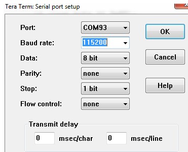
Figure 11. Setting parameters for COM port.
- Set data logging to file from File à Chose the right file.
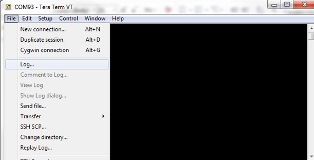
Figure 12. Setting up data logging into file.
- Keep Tera Term opened to see the data written out by another driver.
- The data log file should have all the data captured by the part now.
Now that the data has been logged into data.txt, make sure that there is no incomplete or garbage data at the beginning of the file. This can be due to the data logging that began in the middle of a read.
Python script:
Next, run this python script to read the file and convert each data points into voltage. Also, it plots the logged signal.
"""
Created on Thu Mar 16 15:04:50 2017
@author: MSajikumar
"""
# read each line of file
# into string of 10 characters
# group them in 2s and convert to hex numbers.
import matplotlib.pyplot as plt
def code_to_voltage(code, vref):
voltage = code * 1.0 / 2147483648 * vref
return voltage
voltage_list = []
f = open('teraterm.txt', 'r')
for line in f:
data_string = line
data_string = '0x'+ data_string
print '\nData received: %s' % data_string,
data = int(data_string, 0)
code = data >> 8
last_byte = data & 0xFF
voltage = code_to_voltage(code, 5)
print 'Voltage calculated: %f V' % voltage
voltage_list.append(voltage)
if (last_byte == 0x85):
DF = 256
elif (last_byte == 0xA5):
DF = 1024
elif (last_byte == 0xC5):
DF = 4096
elif (last_byte == 0xE5):
DF = 16384
else:
DF = 0
print 'DF : %d' % DF
plt.plot(voltage_list)
plt.axis([0, 500, -5, 5])
plt.xlabel('Samples')
plt.ylabe('Voltage (V)')


