How To Perform Accurate Measurement and Reduction of Glitch Impulse Energy in DACs
要約
This application note discusses the cause of glitch impulse energy in DACs and suggests a simple solution to reduce it.
Introduction
All digital-to-analog converters (DACs) exhibit a glitch impulse at the analog output when the digital code input changes either from low to high or high to low. This phenomenon is most pronounced during a major carry code transition at midscale, which could create undesirable performance. This application note investigates the cause of this glitch impulse and investigates a practical way to reduce it in a DAC such as the MAX5134, a low-power, 16-bit buffered voltage-output, high-linearity DAC.
What Causes Glitch Energy?
When the DAC output analog value changes, a dynamic phenomenon is observed at the DAC output in the form of a glitch as shown in Figure 1. This glitch energy is defined as the area under the curve on a voltage vs. the time plot as captured on a scope. The unit of this glitch energy is nV × s.
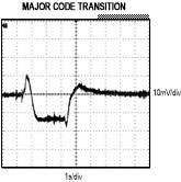
Figure 1. Typical DAC glitch impulse at major code transition.
This glitch is generated due to the mismatched propagation delays among internal switches in selecting the resistors when the digital bits are changed as shown in Figure 2. It is most noticeable when the input code changes at midscale. For a 16-bit DAC like the MAX5134, this code change is from 0X7FFF to 0X8000 or vice versa. The reason is that in binary format, 0X7FFF is 0111 1111 1111 1111 and 0X8000 is 1000 000 0000 00000, respectively. In numeric representation, they are 32767 and 32768, respectively. This shows that at midscale all the bits including the most significant bit (MSB) are changed with only 1 least significant bit (LSB) change, creating a major carry transition because all the internal switches are either open or closed simultaneously. Hence, the worst glitch is generated at this midscale transition.
This glitch can also appear at the output buffer amplifier if it is available in the DAC, as is the case with the MAX5134. The glitch is inherent in all DACs, but its amplitude can be reduced with an external circuitry such as a simple RC low-pass filter.
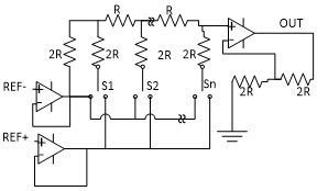
Figure 2. Typical R2R DAC architecture.
Method to Reduce Glitch Impulse
Figure 3 is the scope plot showing the MAX5134 glitch impulse when the input code was changed from 0 to 1. The glitch impulse is barely noticeable because only one internal switch was closed as the input was varied from input digital code 0 to 1.
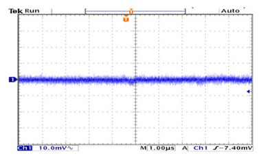
Figure 3. MAX5134 glitch impulse when input digital code was changed from 0 to 1.
Figure 4 is the scope plot showing the MAX5134 glitch impulse when the input code was changed 1LSB at midscale from 0X777 to 0X8000.
As predicted, the glitch impulse is much more pronounced.
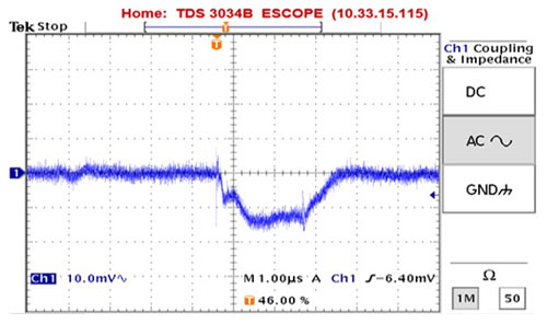
Figure 4. MAX5134 major code transition analog glitch impulse when input code was changed 1LSB from 0X7FFF to 0X8000.
The major code glitch impulse is typically the area under the glitch impulse. It is calculated as follows: Major code transition analog glitch impulse ~ 10mV × 2.5µs ~ 25nV × s, which is specified in the Electrical Characteristics table of the MAX5134 data sheet.
This major code glitch impulse amplitude can be reduced by implementing an RC low-pass filter (R = 13.8k?, C = 33pF) at the output of the MAX5134 DAC as shown in Figure 5.
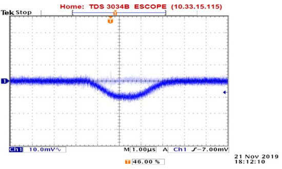
Figure 5. MAX5134 major code transition analog glitch impulse when input code was changed from 0x7FFF to 0x8000 with an RC low-pass filter at the output (R = 13.8k?, C = 33pF).
Major code transition analog glitch impulse with an RC low-pass filter is ~ 10mV × 1.5µs~15nV × s.
This major code glitch impulse amplitude can be reduced further by increasing the capacitor to 100pF at the output of the MAX5134 DAC as shown in Figure 6.
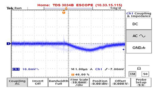
Figure 6. MAX5134 major code transition analog glitch impulse when input code was changed from 0x7FFF to 0x8000 with an RC low-pass filter at the output (R = 13.8k?, C = 100pF).
Major code transition analog glitch impulse with an RC low-pass filter (C = 100pF) is ~ 3 × 1µs × 8mV/2 = 12nV × s.
When C was increased even further to 180pF, the glitch impulse was only 7.5nV × s as captured by the scope plot in Figure 7.
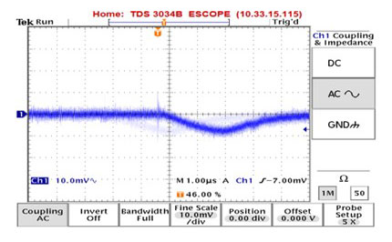
Figure 7. Increasing capacitor value to 180pF to reduce the glitch impulse even further.
Major code transition analog glitch impulse with an RC low-pass filter (C = 180pF) is 3 × 1µs × 5mV/2 = 7.5nV × s.
Table 1 summarizes the glitch impulse energy values with various output low-pass filter bandwidths. As the bandwidth of the RC filter is reduced, the glitch impulse is also reduced. This RC filter bandwidth is chosen to meet the required operating frequency determined by the specific application.
| Bandwidth (kHz) |
Glitch Max (nV × s) |
| — |
20 |
| 349 |
15 |
| 115 |
12 |
| 64 |
7.5 |
Measurement Accuracy
The glitch impulse typically exhibits low amplitude in mV. To measure this low voltage signal accurately, use a Tektronix® P6243 1GHz FET probe. It has 1pF capacitance and high impedance of 1M?. The probe also provides a short connection to ground, enabling more accurate measurement of this glitch impulse energy. Figure 8 and Figure 9 show the desired probe and the MAX5134 glitch impulse measurement setup for accurate measurement.
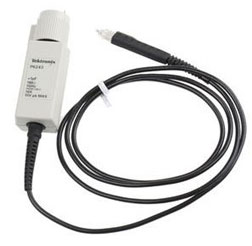
Figure 8. Tektronix P6243 probe.
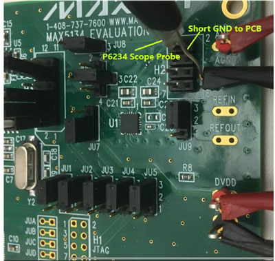
Figure 9. MAX5134 glitch impulse measurement using a Tektronix P6234 probe.
Using other low-frequency probes with long ground connection could yield inaccurate and noisy results as shown in Figure 10 and Figure 11.
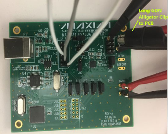
Figure 10. MAX5134 glitch impulse measurement using a standard scope probe with a long alligator clip ground connection to the PCB.
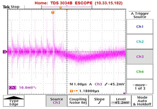
Figure 11. MAX5134 glitch impulse measurement using the same setup conditions as in Figure 7 but with a standard scope probe with long alligator ground clip connection to the PCB.
Conclusion
Glitch impulse energy is inherent in all DACs, but its amplitude can be easily reduced more than 60% by a simple low-pass filter. Since its amplitude is of low signal in mV, it is important that a proper scope probe with a short ground connection to the PCB be used for accurate measurement.


