Effects of Digital Crosstalk in Data Converters
Part 2: Crosstalk on the Clock
Part 2: Crosstalk on the Clock
Part 2 of a series of articles explaining the effects of digital crosstalk in data converters. This article talks about noise on the clock source (jitter) and the effects on the analog-to-digital converter (ADC).
This is Part 2 of a 3-part series:
What is the effect of crosstalk from the digital data signals into the clock signal of a data-conversion system? This is a more obscure problem than crosstalk from digital bits into the analog signal path, which was the subject discussed in the previous article: Part 1 of this series, Effects of Digital Crosstalk in Data Converters.
Data sheets for data converters frequently mention that it is important to minimize crosstalk onto the data converter clock. When asked what happens when it is present, many engineers have the insight that "it creates noise". While this is generally a true statement, there is value to understanding this at a deeper level, so that a design engineer can more efficiently understand and troubleshoot a circuit with this type of problem.
After reading this article, the reader will understand how harmonic distortion and other signal-dependant-error problems can be caused by crosstalk from digital data signals onto the clock. These can take a long time to diagnose and fix if the mechanisms are not understood.
Understanding the concepts from the first article in this series will be helpful to understand before reading this article.
Before we discuss what digital-bit crosstalk can do to a data converter system, it is important to understand what general effects clock noise has on a data converter system.
A data converter clock signal seems like a digital signal. How can it be susceptible to crosstalk?
The clock signal marks a point in time - the point where it crosses a digital signal threshold. If the rise/fall/transition time were zero, then the sampling instant would be precisely defined, despite any noise in the environment. But a real-world clock has slope in its rise and fall. During this transition period, the clock signal is analog. If there is any voltage crosstalk during the slew period near the threshold crossing, it can alter the point in time that the threshold is crossed. This creates a noise on the clock, which is commonly referred to as jitter.
Noise on a data converter clock affects the point in time that the sample of the analog signal of a data converter (i.e., ADC input) is taken. If the analog signal is changing with time, then a different voltage will be sampled than the one originally intended.
The time error (i.e., the jitter) is a function of the slew rate of the clock transition, irrespective of the frequency. This is often a surprise. To quantify: the error in the sampled voltage is the slope of the input signal voltage with respect to time, times the time error.
Dv = (Dv/Dt) × Dt = Slope × Dt
Note that the relationship is independent of the clock frequency. The only things that matter are the picoseconds of jitter on the clock, and the slew rate of the analog signal.
There are many important implications to the above equation that will be discussed below.
Another way of looking at this noise is to look at the signal being sampled as a function of time. i.e.,
X (t) = sin (f × t).
The time component is replaced the by a general jittered time component.
X jittered (t) = X (t + jitter)
For a simple case, we can assume the jitter is a sinusoid.
Jitter = c × sin ( fj × t )
Which would yield the result:
X jittered (t) = sin (f × [ t + c × sin (fj × t) ] )
Note that this is the same equation as a phase modulated (PM) signal. A sine wave with phase modulation is one in which the sine wave is modulated in its phase / timing position. If an ADC were sampling a sine wave modulated at Fj with a pure clock, it would produce the same set of samples as if the ADC were sampling a pure sine wave with a clock whose sample position was jittered at the rate of Fj.
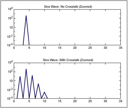
The net effect of a phase modulated or sinusoidally-jittered sine wave is that sidebands show up around the sine wave at the distance of the modulation frequency and its harmonics. As an example, Figure 1 shows a pure sine wave at a frequency of 4, and a similar sine wave at a frequency of 4 with PM modulation/jitter at a frequency of 2. Note that noise components show up at side bands at frequencies of 2 and its harmonics. Or, to give precise numbers: "the sine wave frequency" ±N × "the modulation frequency" or 4 - 2 = 2, 4 + 2 = 6, 4 + 2 × 2 = 8, 4 + 3 × 2 = 10, etc.

Figure 1. A pure sine wave at a frequency of 4, and the same sine wave with PM modulation at a frequency of 2 (which is equivalent to crosstalk onto the clock at a frequency of 2).
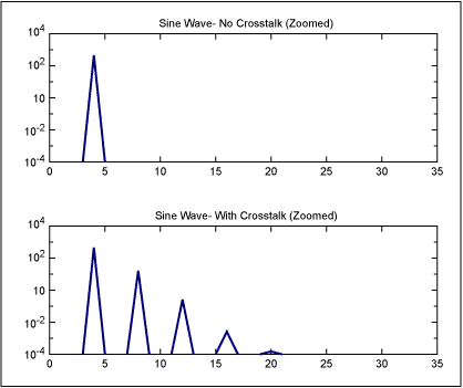
Now, lets look at a more special case of the above: when the crosstalk/phase modulation is at the same frequency as the original signal. The answer follows the same principle and pattern from above. Sidebands appear at a frequency distance of the crosstalk frequency and its harmonics. Figure 2 shows such an example: a sine wave at a frequency of 4, with PM modulation/clock noise at a frequency of 4. Note that the sidebands appear at frequencies of 4 + 4 = 8, 4 + 2 × 4 = 12, 4 + 3 × 4 = 16, etc.
Could you distinguish this from harmonic distortion?

Figure 2. A pure sine wave at a frequency of 4, and the same sine wave with PM modulation at a frequency of 4 (which is equivalent to crosstalk onto the clock at a frequency of 4).
Why did we analyze this obscure case? Because this is directly related to what happens when there is crosstalk from the digital data signals from an ADC onto its clock. The noise source is the digital data signal energy. Due to the capacitive coupling mechanisms this energy results in sinusoidal "noise" on the clock at the same frequency as the clock. This important concept is addressed in detail in Part 3 of this article series, Effects of Digital Crosstalk in Data Converters, Part 3: Digital Data Signal Crosstalk on the Clock.