要約
Industry 4.0 is moving industrial automation technology closer to the edge of the factory floor. In this design solution, we show how the MAX22513 surge-protected IO-Link® transceiver with an integrated DC-DC converter reduces power dissipation and component area in high-current industrial sensors.
Every revolution worthy of the name deserves an equally worthy motto. “Liberty, Equality, Fraternity” was chosen by the French. The Fourth Industrial Revolution (thankfully without bloodshed or strife) could potentially have a greater global impact on the lives of people than any political revolution. It could be argued that “Intelligence, Adaptability, Efficacy” might make a suitable catchphrase for Industry 4.0 (Figure 1), as this revolution is regularly alluded to.

Figure 1. Industry 4.0 or the Fourth Industrial Revolution.
Whether you deem it a worthy slogan or not, it cannot be disputed that each of these terms is applicable to IO-Link® technology, which is at the vanguard of this industrial revolution and is facilitating smarter, more adaptable, and increasingly efficient industrial sensors on the factory floor. For industrial system designers, the relentless challenge is to ensure that this increased performance does not come at the expense of increased power or heat dissipation and consequently increased sensor size. In this design solution, we review the power constraints when designing high-current, small-enclosure IO-Link sensors that operate in harsh, fanless industrial environments. After considering the compromises encountered with incumbent solutions, we present a new IO-Link transceiver IC that overcomes these limitations while simultaneously increasing design flexibility and improving sensor robustness.
What is IO-Link?
IO-Link is a standardized technology (IEC 61131-9) that regulates how sensors and actuators in industrial systems interact with a controller. It is a point-to-point communication link with standardized connectors, cables, and protocols. The IO-Link system is designed to work within the industry-standard 3-wire sensor and actuator infrastructure and is comprised of “IO-Link master” and “IO-Link device” products (Figure 2).
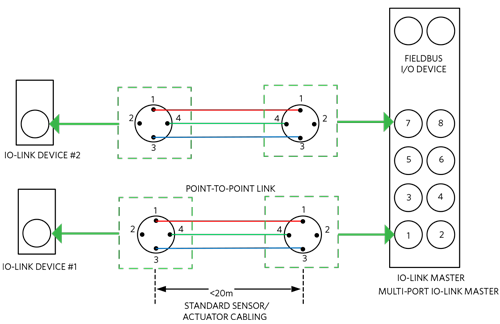
Figure 2. IO-Link Master/Device Interface.
Pins 1 (L+, 24V) and 3 (L-, 0V), are for power while pin 4 (C/Q) carries communication or switching information as required. Pin 2 can remain unconnected (NC) or it can be configured for use as a digital input (DI) or digital output (DO) to provide switching information while the C/Q pin is used to transfer data to/from an IO-Link sensor. The IO-Link standard states that communications must be within 20 meters with unshielded cables using standard connectors common to industrial systems. Communication between master and slave devices is half-duplex with 3 transmission rates: COM1 4800 baud, COM2 38.4k baud, COM3 230.4k baud. The IO-Link device only supports one data rate while the IO-Link master must support all three data rates.
IO-Link Sensor Design
Most industrial sensors use either an M8 or a larger M12 (Figure 3) cable connector. The type of connector used will impact the enclosure size of the sensor and therefore the amount of heat that can be dissipated. In the following example, we will design an IO-Link sensor with a total power dissipation that will not exceed 400mW if an M8 connector is used, or 600mW for a sensor using an M12 connector.
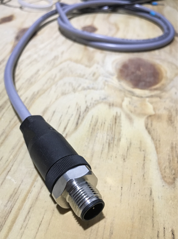
Figure 3. M12 Sensor Connector.
Apart from a transducer (pressure/temperature/proximity), an IO-Link industrial sensor will also typically include an analog front-end (AFE), a microcontroller, status LEDs, and possibly an output stage to drive an actuator in response to sensor readings. Industrial sensors use a 24VDC signal voltage, but in a harsh factory environment, this can be up to 50% higher. While these voltage levels can be safely used to power the output driver stage, the AFE, LEDs, and microcontroller require much lower voltages (3V to 5V) for operation. Many IO-Link transceivers provide these voltage levels as linear regulated outputs. However, the decision to use them can have negative implications for overall sensor power consumption (and consequently, heat dissipation). This is especially true if an inefficient onboard LDO circuit is used to provide the current for these outputs. For example, consider the following power budget for a small sensor drawing just 15mA of current through an LDO, powered from a (typical) 30V DC rail, shown in Figure 4.
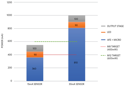
Figure 4. Power Budget (mW) for Typical IO-Link Sensors.
Due to the high losses inside the LDO this relatively low power sensor has exceeded the ~400mW power-budget that can be dissipated in a typical M8 connected sensor, and therefore, a larger M12-connected enclosure would be required. The figure also shows that a sensor drawing just 30mA of current will dissipate 900mW, exceeding even the target figure for an M12 connector sensor.
Conventional Solution
To reduce overall power consumption (and heat dissipation), the most common solution is to use an external DC-DC buck converter to power the linear regulators on the transceiver. For example, a DC-DC buck converter supplying a 30mA sensor with a 3V output voltage will dissipate just 90mW. Assuming the converter is 90% efficient (i.e. just 9mW power loss), the overall power consumption is just 90 + 9 = 99mW. Clearly, power dissipation is reduced by approximately a factor of 9 when compared to using the LDO (900mW). Including the power consumed by the output stage (100mW), the overall power reduction would be 1000mW/199mW, or approximately a factor of 5, as shown in Figure 5.
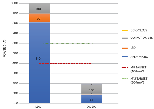
Figure 5. Power Reduction Using a Buck Converter vs. LDO.
Clearly, the overall power consumption of the sensor (~200mW) is now well below the target figure for sensors using either type of connector. However, this power reduction is only achieved at the expense of extra external circuitry (i.e. the DC-DC converter and bulky discrete items such as an inductor, diodes, and capacitors), which increases the overall size of the sensor. A typical IO-Link transceiver solution would require a component area of 16.5mm2 as shown in Figure 6, with the DC-DC converter consuming more area than the IO-Link transceiver itself. To protect against voltage surges, some transceivers may additionally require external TVS diodes, further increasing component (and board) area.
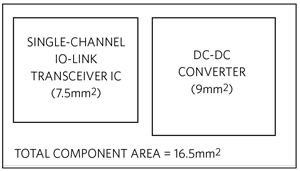
Figure 6. Typical IO-Link Transceiver Solution.
Integrated Dual-Channel Transceiver
The IO-Link transceiver IC shown in Figure 7 has several advantages when compared to the conventional approach. Firstly, a reverse polarity protected Buck DC-DC converter has been fully integrated into the IC package, meaning a separate DC-DC converter IC is not required. The converter can supply an output current of up to 300mA (for high-current sensor applications) with a 2.5V to 12V programmable output voltage. Secondly, unlike most other IO-Link transceivers, the IC also includes a second (dual) IO-Link channel which can be used for DI/DO sensor switching while data is being transferred on the C/Q channel. Despite the inclusion of these extra features, the overall package size is only 2.1 × 4.1 = 8.6mm2 in a WLP. This represents an almost 50% reduction in component area. Additionally, robust sensor performance in harsh industrial environments is provided by integrated surge protection (up to 1kV/500O) circuitry that negates the need for external TVS diodes.
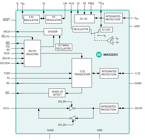
Figure 7. MAX22513 Dual-Channel IO-Link Transceiver.
Conclusion
In this design solution, we have reviewed the power constraints when designing IO-Link sensors for harsh, fanless industrial environments. We have shown that using an LDO to supply sensor current is not always a viable option for high current sensors as it greatly increases power consumption. Until now, the only solution available to reduce heat dissipation was to use a separate DC-DC buck converter IC, but this came with the caveat of increasing overall sensor size. However, the MAX22513 surge-protected dual-driver IO-Link device transceiver now provides a fully integrated alternative for high-current sensors, providing greater flexibility, combined with robust performance, in a much smaller form factor.
Learn more:


