製品概要
機能と利点
- Supply voltages
- Dual-supply: ±5 V to ±22 V
- Single-supply: 8 V to 44 V
- Protected against overvoltage on the device source pins (S and SFB) on Terminal J2
- Protected against signal voltages up to ±60 V
- LEDs for visual overvoltage indication
- Parallel interface compatible with 1.8 V logic
- On-board LDO regulator for digital supply and control, if required
製品概要
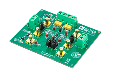
The EVAL-ADG5401FEBZ evaluation board for the ADG5401F features one SPST switch channel and one feedback switch channel. The ADG5401F SPST switch has overvoltage detection and protection circuitry on the source pins (S and SFB) on Terminal J2 and is protected against signals up to ±60 V in the powered state and unpowered state.
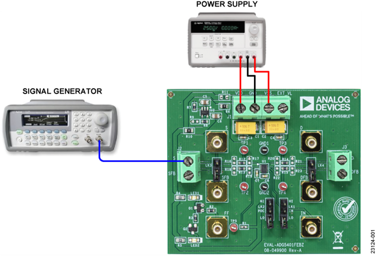
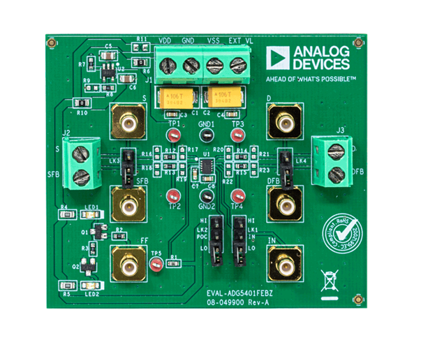
Figure 1 shows the EVAL-ADG5401FEBZ in a typical evaluation setup. The ADG5401F is soldered to the center of the EVALADG5401FEBZ, and two wire screw terminals (J2 and J3) are provided to connect to each device source pin (S and SFB) and drain pin (D and DFB). The J1 screw terminal powers the device through three EVAL-ADG5401FEBZ supply pins (VDD, GND and VSS), and a fourth pin (EXT_VL) provides a user defined digital voltage of 1.8 V to 5 V, if required. Alternatively, a low dropout (LDO) regulator (ADP7142) is provided for 5 V digital voltage control and to supply both light emitting diodes (LEDs) LED1 and LED2, which are mounted to provide visual indication of the fault status of the switch.
For full specifications on the ADG5401F, see the ADG5401F data sheet, which must be consulted in conjunction with the user guide when using the EVAL-ADG5401FEBZ.
マーケット&テクノロジー
対象となる製品
パッケージの内容
EVAL-ADG5401FEBZはじめに
DOCUMENTS NEEDED
- ADG5401F data sheet
EQUIPMENT NEEDED
- DC voltage source
- ±5 V to ±22 V for dual supply
- 8 V to 44 V for single supply
- Optional digital voltage source: 1.8 V to 5 V
- Analog signal source (signal generator)
