Design Note 68: New Synchronous Stepdown Switching Regulators Achieve 95% Efficiency
The new LTC1148 and LTC1149 synchronous switching regulator controllers make high efficiency DC/DC conversion possible in a wide range of applications. These controllers share a current-mode architecture which combines synchronous switching for maximum efficiency at high currents with an automatic low current operating mode, called Burst Mode® operation, which makes 90% efficiencies possible at output currents as low as 10mA.
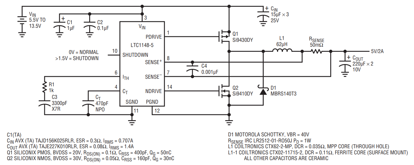
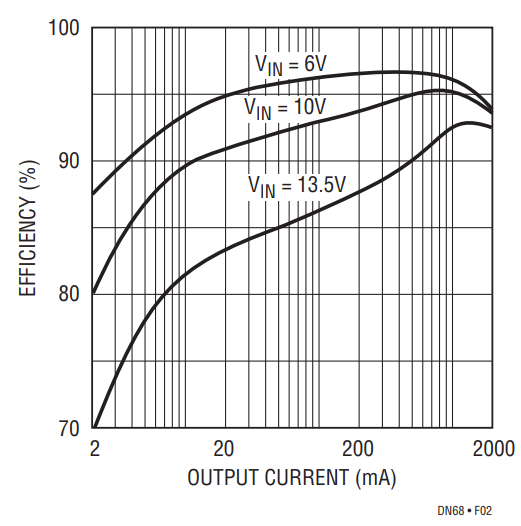
Figure 1 shows a typical LTC1148 surface mount application providing 5V at 2A from an input voltage of 5.5V to 13.5V. The operating efficiency, shown in Figure 2, peaks at 97% and exceeds 90% from 10mA to 2A with a 10V input. Q1 and Q2 comprise the main switch and synchronous switch, respectively, while inductor current is measured via the voltage drop across current shunt RSENSE. RSENSE is the key component used to set the output current capability according to the formula IOUT = 100mV/RSENSE. Advantages of current control include excellent line and load transient rejection, inherent short-circuit protection and controlled start-up currents. Peak inductor current is limited to 150mV/RSENSE or 3A for the Figure 1 circuit.

Figure 1. LTC1148 (5.5V-13.5V to 5V/2A) Surface Mount.

Figure 2. LTC1148-5: 5.5V TO 13.5V Efficiency.
The timing capacitor, CT, sets the off-time according to the formula tOFF = 1.3 • 104 • CT. The constant off-time architecture maintains a constant inductor ripple current, while the operating frequency varies with input voltage. The Figure 1 circuit has an off-time of approximately 6μs, resulting in an operating frequency which varies from 60kHz to 90kHz over an 8V to 12V input range.
When the output current drops below approximately 15mV/RSENSE, the LTC1148 automatically enters Burst Mode operation to reduce switching losses. In this mode, the LTC1148 holds both MOSFETs off and sleeps at 200μA supply current, while the output capacitor supports the load. When the output capacitor discharges 50mV, the LTC1148 briefly turns back on, or “bursts,” to recharge the capacitor. The timing capacitor Pin 4, which goes to 0V during the sleep interval, can be monitored with an oscilloscope to observe burst action. You will observe the circuit bursting less and less frequently as the load current is reduced. Complete shutdown reduces the supply current to only 10μA.
For applications which require greater than 13.5V, the higher voltage LTC1149 includes all of the operating features of the LTC1148 plus an internal regulator and a gate drive level shift circuit which allow operation up to VIN = 48V. The design and performance of an LTC1149 based circuit is similar to that of the Figure 1 LTC1148 circuit, with a slight increase in sleep current (600μA) and shutdown current (150μA) due to the additional LTC1149 high voltage circuitry.
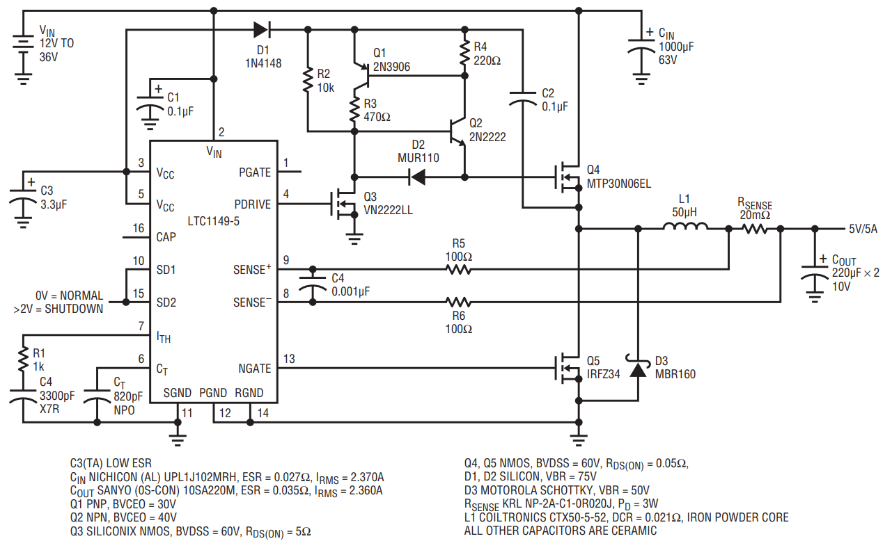
Although highly efficient at output currents of under 2A, P-channel MOSFETs can become a dominate loss element at higher output currents, limiting overall circuit efficiency. Consequently, N-channel MOSFETs are better suited for use in high current applications because they have a substantially lower ON resistance. The circuit shown in Figure 3 utilizes the low loss characteristics of N-channel MOSFETs, providing efficiency in excess of 90% at an output current of 5A.
Figure 3’s operation is similar to that of the Figure 1 circuit, but it utilizes an LTC1149, which accommodates higher input voltages, and has been modified to drive the top N-channel MOSFET. The circuit operation is as follows: the LTC1149 provides a PDRIVE output (Pin 4) that swings between ground and 10V which turns Q3 on and off. While Q3 is on, the N-channel MOSFET (Q4) is off because its gate is pulled low by Q3 through D2. During this interval, the NGATE output (Pin 13) turns the synchronous switch (Q5) on, creating a low resistance path for the inductor current.

Figure 3. LTC1149-5 (12V-36V to 5V/5A) Using N-Channel MOSFETs.
In order to turn Q4 on, its gate must be driven above the input voltage. This is accomplished by bootstrapping capacitor C2 off the source of Q4. The LTC1149 VCC output (Pin 3) supplies a regulated 10V output that is used to charge C2 through D1 while Q4 is off. With Q4 off, C2 charges to 5V for the first cycle in Burst Mode operation and 10V thereafter.
When Q3 turns off, the N-channel MOSFET is turned on by the SCR connected NPN-PNP (Q1 and Q2) network. Resistor R2 supplies Q2 with enough base drive to trigger the SCR. Q2 then forces Q1 to turn on which supplies more base drive to Q2. This regenerative process continues until both transistor are fully saturated. During this period, the source of Q4 is pulled to the input voltage. While Q4 is on, its gate source voltage is approximately 10V, fully enhancing the N-channel MOSFET.
