

AN-1536: APTMC120AM20CT1AG SiC パワー・スイッチを駆動するADuM4135 ゲート・ドライバの性能
はじめに
太陽光発電(PV)やエネルギー貯蔵などのアプリケーションにおいては、これまで求められてきた効率向上の必要性に加え、電力密度が増大する傾向にあります。この問題に対するソリューションが、シリコン・カーバイド(SiC)パワー・デバイスの形となって現れています。SiC デバイスはワイド・バンドギャップ・デバイスで、DC 動作電圧を 1000 V 以上に上げることが可能で、ドレイン・ソース・インピーダンス(RDSON)も低くすることができます。また SiC デバイスは、絶縁性を上げ、それにより効率を向上させるというニーズにも応えます。さらに、SiC デバイスは寄生容量が小さく、それによるスイッチング時の電荷量も少ないため、100 kHz を上回る高速スイッチング速度を示します。しかし、短所の 1 つとして、ゲート・ドライバには 100 kV/μs を超える高いコモンモード過渡耐圧(CMTI)が必要となります。また、SiC のドレイン・ソース間の高速スイッチングによりデバイスのゲートでリンギングが発生する可能性があるという短所もあります。SiC を実装することで著しく電力密度が改善できる状況において SiC デバイスを高電圧で駆動する場合、このような短所によって問題が発生する可能性があります。この問題を解決できるゲート・ドライバと SiC の組み合わせの 1 つが、ADuM4135 と Microsemi 製APTMC120AM20CT1AG モジュールです。ADuM4135 ゲート・ドライバは、25 V の動作電圧(VDD・VSS 間電圧)時に 7 A(代表値)のソースおよびシンク電流駆動能力を持つ 1 チャンネル・デバイスです。CMTI の最小値は 100 kV/μs です。APTMC120AM20CT1AG パワー・モジュールは、ハーフ・ブリッジ SiC デバイスで、1200 V(定格値)のコレクタ・エミッタ電圧、17 mΩ の RDSON、108 A の直流駆動電流の性能を示します。ゲート・ソース間電圧(VGS)の定格は、−10 V ~ +25 V です。

試験構成
電気的構成
システムの試験回路構成を図 2 に示します。DC 電圧がフル・ハーフ・ブリッジ全体の入力に印加されます。入力段には 900 μFのデカップリング・コンデンサが付加されています。出力段は、83 μH と 128 μF のインダクタ・コンデンサ(LC)フィルタ段で、ここでフィルタリングを行って 2 Ω ~ 30 Ω の負荷 R1 に出力します。

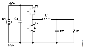
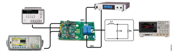
表 1 に試験構成の電力部品を示します。具体的な構成を図 3 に示します。表 2 には試験で使用した装置構成の詳細を示します。
| Equipment | Value |
| U1 | 200 V to 900 V |
| C1 | 900 μF |
| L1 | 83 μH |
| C2 | 128 μF |
| R1 | 2 Ω to 30 Ω |
| Equipment | Manufacturer | Type |
| Oscilloscope | Keysight | DSO-X 3024T |
| DC Supply | Delta Elektronika | SM 660-AR-11 (two in serial) |
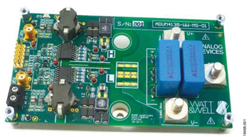
| Gate Driver Board | Watt&Well | ADUM4135-WW-MS-01 SN001 |
| Waveform Generator | Agilent | 33522A |
| Current Probe | Hioki | 3275 |
| Passive Voltage Probe | Keysight | N2873A 500 MHz |
| Passive High Voltage Probe | Elditest | GE3421 100 MHz |

テスト結果
無負荷試験
| Test | VHV (V)1 | Switching Frequency, fSW (kHz) | Duty Cycle (%) | IIN (A)2 | Figures |
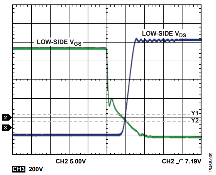
| 1 | 600 | 50 | 50 | 0.26 | 図 4 and 図 5 |
| 2 | 600 | 100 | 50 | 0.22 | 図 6 and 図 7 |
| 3 | 900 | 50 | 50 | 0.37 | 図 8 and 図 9 |
1 VHV は HV+ と HV− の間の差動電圧。
2IIN は U1 を流れる入力電流。
| Test | VHV (V) | fSW (kHz) | Ambient Temperature (°C) | Heatsink Temperature (°C) | DC-to-DC Power Supply Temperature, High-Side (°C) | DC-to-DC Power Supply Temperature, Low-Side (°C) | Gate Driver Temperature, High-Side (°C) | Gate Driver Temperature, Low-Side (°C) |
| 4 | 600 | 50 | 20 | 21.3 | 25.4 | 25.4 | 34 | 33.5 |
| 5 | 600 | 100 | 20 | 23.5 | 31.5 | 31.5 | 42 | 42 |
| 6 | 900 | 50 | 20 | 23 | 29 | 29 | 37 | 37 |
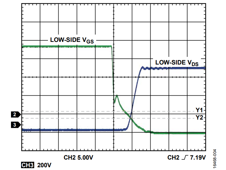
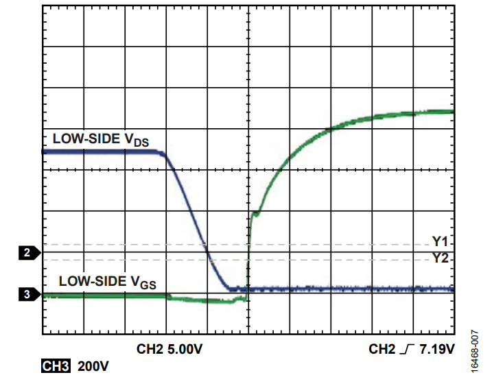
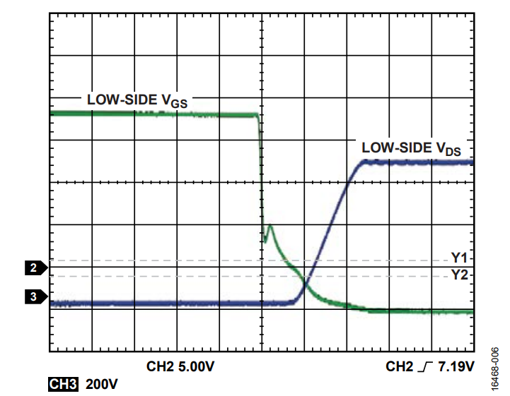
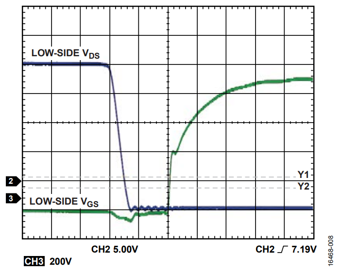
ADuM4135 の最新バージョンには、変更点がいくつかあります。2.2 nF のコンデンサが、パワー MOSFET(金属酸化物半導体電界効果トランジスタ)Q1 と Q2 に追加されました。また、15 nFの C0G デカップリング・コンデンサが VHV に追加されています。表 3 と表 4 に測定結果をまとめます。図 4 ~ 図 9 は結果をグラフで示したものです。試験 1 と試験 2 は 600 V で行ったもので、スイッチング周波数はそれぞれ 50 kHz と 100 kHz です。これに対し、試験 3 は 900 V、スイッチング周波数 50 kHz で行ったものです。


負荷試験
| Test | VHV (V) | fSW (kHz) | Duty Cycle (%) | IOUT1 (A) | VOUT2 (V) | POUT3 (W) | IIN4 (A) |
Figures |
| 4 | 200 | 50 | 25 | 1.7 | 48 | 83 | 0.55 | Figure 10 and Figure 11 |
| 5 | 600 | 50 | 25 | 6.9 | 145 | 1000 | 1.66 | Figure 12 and Figure 13 |
| 6 | 900 | 50 | 25 | 8.7 | 215 | 1870.5 | 2.47 | Figure 14 and Figure 15 |
| 7 | 900 | 100 | 25 | 8.2 | 200 | 1640 | 2.13 | Figure 16 and Figure 17 |
1 IOUT は負荷抵抗 R1 を流れる出力電流。
2 VOUT は R1 に印加される出力電圧。
3 POUT は出力電力(IOUT × VOUT)。
4 IIN は U1 を流れる入力電流。
基板の構成は、無負荷試験のセクションで説明した試験構成と同様です。
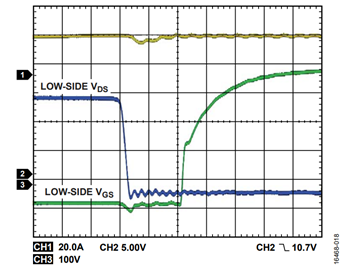
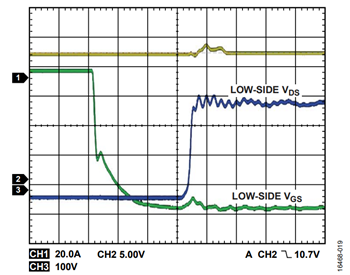
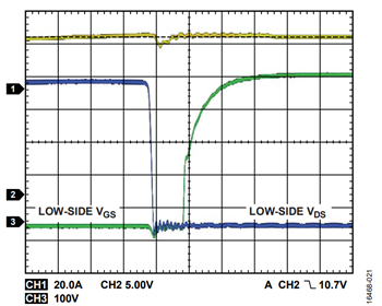
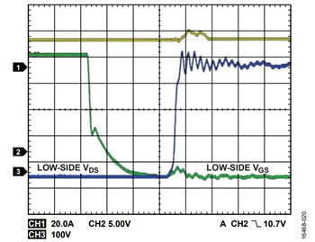
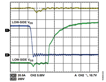
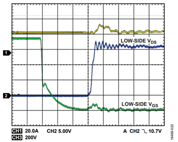
表 5 に負荷試験の測定結果をまとめます。図 10 ~ 図 17 は結果をグラフで示したものです。

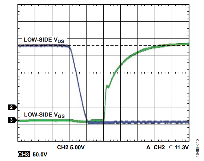

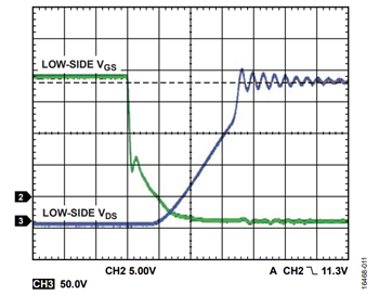

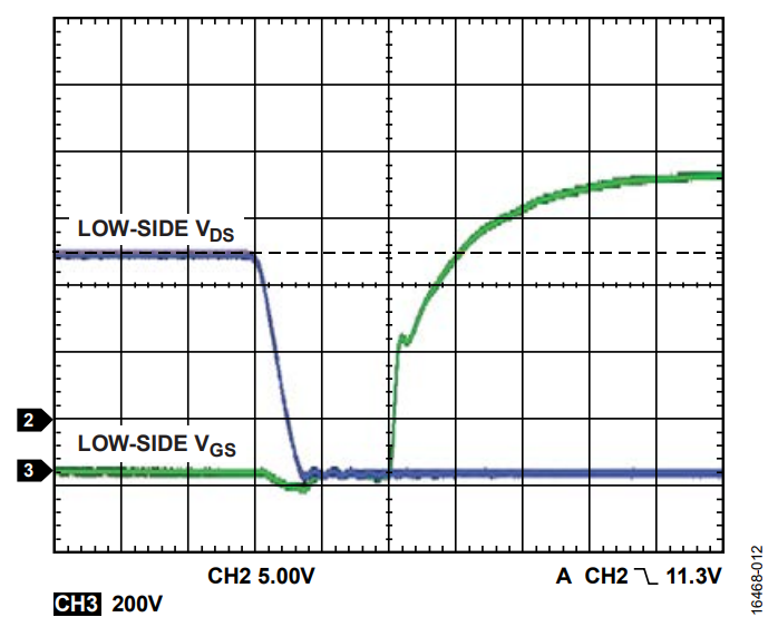

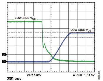

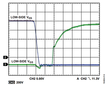

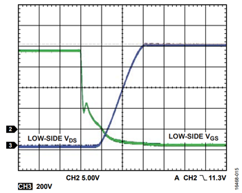

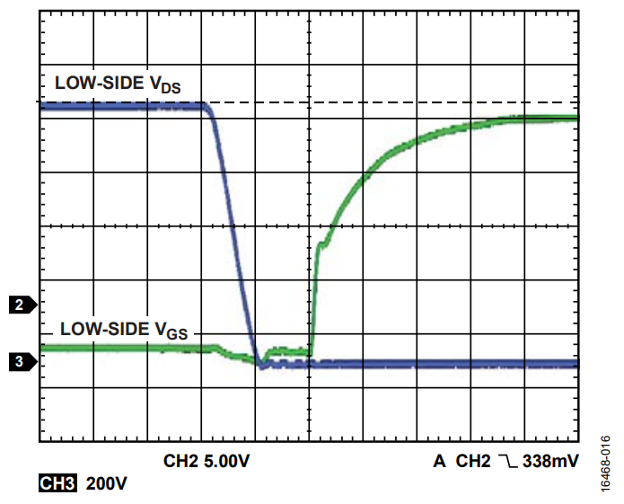

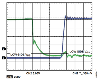
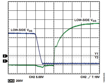
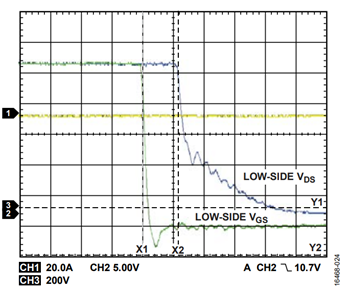
出力電圧(VOUT)は R1 の両端の電圧を測定したものです。この試験結果は、VGS に若干のミラー効果が表れることを示していますが、VGS は SiC のゲートにおいて -5 V のレベルを維持しています。900 V のときは、VDS にある程度のリンギングが見られますが、入力 DC 電圧の 100 V を下回っています。この設計によって、ADuM4135 が SiC MOSFET を駆動するのに問題のない性能を持っていることがわかります。
高電流試験
| Test | VHV (V) | fSW (kHz) | Duty Cycle (%)1 | IOUT2 (A) | VOUT3 (V) | PIN4 (W) | IIN5 (A) | Figures |
| 4 | 300 | 50 | 25 | 21.8 | 70.14 | 1526 | 5 | Figure 18 and Figure 19 |
| 5 | 400 | 50 | 25 | 27.1 | 93.8 | 2640 | 6.6 | Figure 20 and Figure 21 |
| 6 | 600 | 50 | 25 | 40.5 | 141 | 6000 | 10 | Figure 22 and Figure 23 |
1 デューティ・サイクル・ハイ・サイド。
2 IOUT は負荷抵抗 R1 を流れる出力電流。
3 VOUT は R1 に印加される出力電圧。
4 PIN は入力電力(IIN × VHV)。
5 IIN は U1 を流れる入力電流。
基板構成は、無負荷試験のセクションで説明した試験構成と同様です。この試験では Regatron の電源を使用しました。
表 6 に高電流試験の測定結果をまとめます。図 18 ~ 図 23 は結果をグラフで示したものです。
VOUT は R1 の両端の電圧を測定したものです。


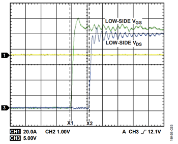
PWM 遅延
ADuM4135 の入力 PWM と出力 PWM とで、入出力信号間の遅延を測定できます。測定は、ADuM4135 の入出力ピンで直接行いました。遅延は 59.4 ns になります。


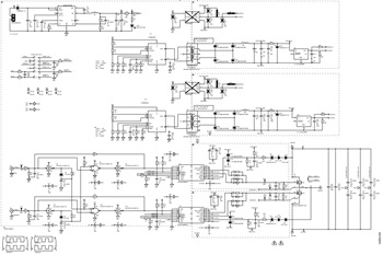
回路図

まとめ
ADuM4135 には電流駆動能力、正確な電源範囲、100 kV/μs を上回る強い CMTI 能力が備わっており、SiC MOSFET を駆動する場合に問題のない性能を発揮します。
この試験結果から、絶縁電源や SiC を駆動する高電圧ゲート・ドライバとして使用可能なソリューションがあることが示されました。
著者
