

AN-1386: サンプル・クロック・スペクトラムが ADC の測定信号スペクトラムに及ぼす影響に関する簡単な数学的説明
はじめに
最近の高速 A/D コンバータ(ADC)の性能は、そのクロックに直接依存しています。しかし、これらのクロックを生成するために使われている信号発生器の発振器は理想的なものではなく、クロックの振幅も位相も理想値から外れています。ADC のサンプリング回路は小さいクロック振幅の変化に影響されない傾向にありますが、位相オフセットの場合は、それが小さいものであっても ADC の出力に大きく影響します。したがって、高速 ADC で正確な値を得ようとする場合は、クロック発振器の位相ノイズを慎重に分析する必要があります。
このアプリケーション・ノートでは、クロックおよびアナログ入力の位相ノイズの影響を理解するために必要な、数学的背景について概要を示します。このような数学的背景は十分に確立されたものですが、実際に使われることは稀です。ここでは、振幅ノイズと位相ノイズの相違点と類似点について述べるとともに、側波帯電力を予測する式について提案を行い、さらにクロックおよびアナログ入力のノイズが測定 ADC 信号に結合するメカニズムを明らかにします。
最後に、AD9684 を例にとり、最近の高速 ADC の評価と性能予測にこれらの手法を適用する方法も示します。
振幅ノイズと位相ノイズの関係
高速 ADC のクロック波形には、ほとんど正弦波が使われています。これは、矩形波などの他の波形よりも、正弦波の方が、生成、伝送、RF 周波数でのマッチングを容易に行えるためです。正弦波は、数学的には次のように記述できます。

ここで、
c(t)はキャリア(クロック)、
Ac はキャリア振幅、
ωc は角周波数、
t は時間です。
通常、クロック信号は高電力であり(>13 dBm)、これが配線やコネクタ、およびパターンによる損失を補います。クロック電力はノイズ電力より高いと見なしても支障はありません。
三角関数の近似
このアプリケーション・ノートでは、全体を通じ、x << 1 の領域では以下の近似が使われています。したがって、ここに示すアプローチが成り立たなくなった場合には何が起こるのかを認識しておくことが重要です。これらの単純な線形近似では、図1 に示すように、x の値が大きくなると誤差も大きくなります。


確定的アプローチ
最初のテーマはクロック・ノイズですが、これは、以下の証明では正弦関数で表せるものと仮定します。この単純化により、キャリアとノイズの間の位相を分析することができます。振幅ノイズは振幅変調(AM)の形で検討します。

ここで、
cAM(t)は AM ノイズを含むキャリア(クロック)、
Ac はキャリア振幅、
An はノイズ振幅、
ωn はノイズの角周波数です。
AM は 2 つの周波数成分を生成することに注意してください。1つはキャリア周波数より低い成分、もう 1 つは高い成分です。したがって、この変調は一般に両側波帯(DSB)変調と呼ばれます。これら 2 つの成分の位相も、キャリアの位相に揃えられます。波形はすべて正弦波です。
図 2 に示す信号のフェーザ図は、位相結合をより直感的に示しています。sinωct のキャリアは 90 ° の位相に位置し、垂直方向(上)を向いています。キャリアを基準として比較すると、2つのノイズ成分は ωn の角速度で互いに反対方向に回った位置になります。したがってその合計は、常にキャリアと同方向のベクトルとなります。言葉を変えると、振幅ノイズは常にキャリアと同位相になります。これらの AM 変調された信号のスペクトラムを図 3 に示します。


次のテーマは、位相変調(PM)の形を取る位相ノイズです。

この場合は、An を位相変調指数と呼ぶことができます。An << 1の場合は次式が成り立ちます。

これにより、PM の式を単純化することができます。

2 つのノイズ成分が、AM-DSB の場合と同じ周波数に現われます。唯一の違いはそれらの位相で、AM-DSB 信号と比べて 90 °ずれています。したがって、その合計は常にキャリアに対して直角です。フェーザ図と信号スペクトラムは、信号可視化の助けとなります(図 4 と図 5 を参照)。


これらの図は、スペクトラム解析におけるひとつの根本的な問題も示しています。それは、AM-DSB 信号と低変調指数 PM 信号のスペクトラムを区別できないことです。多くの場合 AM ノイズと PM ノイズは同時に存在し、測定されたスペクトラムは、それぞれのスペクトラムの組み合わせです。
確率的アプローチ
ノイズは確定的なものではなく、多くの場合は正弦波でもありません。したがって、解析に関する次のトピックは、確率的ノイズのパワー・スペクトラム密度(PSD)です。スペクトラムには負の周波数が含まれていますが、これは、電気通信における信号解析方法の慣習に関係する概念です。
ノイズ関数 n(t)の期待値はゼロ、つまり E[n(t)]= 0 であるものとし、その DSB PSD は ν(ω)、つまり ν(ω)= ν(−ω)であるものとします。
まず、AM ノイズ信号から考えていきます。

そのフーリエ変換を次のように定義したとします。

ここで、T は周期です。
この場合、その PSD の式は次のように表すことができます。
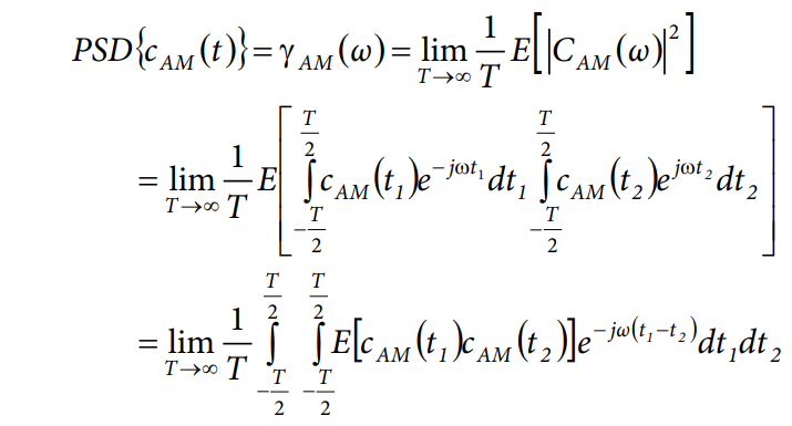
重要な部分は積分内にある期待値の式で、これは個別に扱われます。

変数 t1 と t2 は、τ = t1 − t2 と υ = t1 + t2 に置き換えられます。E[n(t1)n(t2)]は時間差だけに依存すると仮定します。したがって、これは自己相関関数 R(τ)に置き換えることができます。

この結果は、PSD の計算式に代入することができます。多重積分内の変数を変更する場合は、ヤコビ行列の行列値(この場合は 1/2)を式に乗じる必要があります。変数の変更は、積分限界にも影響を与えることに注意してください。

変数 υ に依存するのは(cosωcτ − cosωcυ)だけです。したがって、これは個別に積分することができます。

これにより、PSD の式はさらに簡単になります。

結果は、前の結論に対応します。信号スペクトラムは 2 つの主要部分で構成されます。第 1 の部分は角周波数 ωc の純粋なキャリアで、これは 2 つの「ディラックのデルタ関数」で表されます。すなわち、正の周波数の場合は δ(ω − ωc)、負の周波数の場合は δ(ω + ωc)です。
第 2 の部分はノイズ信号自体の DSB PSD で、やはり ωc にミックスされます(ν(ω − ωc)と ν(ω + ωc)を参照)。これはAc2/4 によってスケーリングされ、スペクトラムのあらゆる絶対測定値はこの係数を包含しています。しかし実際には、このような依存性を避けるために、測定ノイズは測定キャリアに基づいて電力にスケール・バックされて、DC にシフト・バックされます。その結果がオリジナルのノイズ PSD ν(ω)で、ここではこれをキャリア基準ノイズ PSD と呼びます。
次に、位相変調について検討します。

n(t)<< 1 の場合は次式が成り立ちます。

これにより、式を単純化することができます。

その PSD の式は次のように表すことができます。

重要な部分は期待値で、これについては個別に検討します。

第 1 の部分は純粋なキャリアで、これは前に示した証明と同じです。したがって、問題となるのは第 2 の部分だけです。変数t1 と t2 は、τ = t1 − t2 と υ = t1 + t2、および E[n(t1)n(t2)]= R(τ)に置き換えられます。第 2 の部分は次式で表されます。

変数 υ については個別に積分します。

この式を PSD の計算に代入します。

最後に、すべての部分をまとめます。

ここでも、信号スペクトラムが、角周波数 ωc の純粋なキャリアと、ωc にミックスされたノイズ信号自体の DSB PSD から構成されることが分かります。しかしこの場合、ミキシングは、90 ° の位相シフトを追加して余弦により行われます。
結果
確定的フェーザ・アプローチでも確率的アプローチでも、同じように広範な結果になることが分かります。第 1 に、低変調指数の PM 信号では、側波帯は変調指数と直接的な関係があります。側波帯の電力を調べれば、位相ノイズの電力が分かります。
第 2 に、あらゆる追加ノイズ・ベクトルは、AM ノイズ(キャリアと同位相)と PM ノイズ(キャリアと直角)を合計したものと解釈することができます。PM ノイズを対象とする場合、側波帯電力に基づいて位相ノイズ電力を予測できるようにするには、あらかじめ AM 成分を除去する必要があります。
第 3 に、この証明が有効なのは変調指数が低い場合に限られます。それ以外の場合は、側波帯電力と位相ノイズ電力の間に直接的な関係が無くなり、この結論に基づく予測は本質的に無効になります。
低 PM 変調指数の基準
正弦関数と余弦関数をテイラー展開すると、変調指数が高くなった場合にどうなるかが明らかになります。ノイズ関数は非直線領域に入りますが、単純な確定的正弦波ノイズの場合、これは次のようになります。

式内の 3 乗項、5 乗項、および以降の奇数乗項は、追加的な電力を伴う高調波を側波帯内に発生させ、PSD の計算はベッセル積分に変わります。関連する各式は、前述の証明に基づいて容易に記述できますが、これらの式は長く、あまり参考になりません。実際には、側波帯電力が PM ノイズ電力より大きくなり、側波帯電力を使って PM ノイズ電力を予測することができなくなります。しかし、低変調指数と高変調指数の間に明確な境界はなく、この単純な近似がうまく機能するかどうかの判断は、ユーザーに委ねられます。
側波帯電力
スペクトラム・アナライザによって調査した非理想クロックは、1 つの無限に狭いピークではなく、連続的な側波帯を伴っています。この側波帯は、明確な境界なしで徐々にノイズ・フロアまで低下していきます。ここで考えるべき問題には、以下のようなものがあります。
- どこまでの側波帯電力を積分すべきか?
- ノイズ・フロアは側波帯電力の一部か?
2 番目の疑問への答えは簡単です。何らかの入力信号がある場合とない場合のノイズ・フロアを、単純に比較すれば分かります。スペクトラム・アナライザのノイズがクロック・ノイズに影響することはないので、これは無視できます。
最初の疑問については、さらに検討を加える必要があります。まず、ノイズの帯域幅を明らかにしなければなりません。低周波数だけを考慮したくなりますが、信号の高電力 PSD 領域も考慮が必要です。ただし、最終的には広い領域が積分対象になるので、非常に低電力の広帯域ノイズの寄与分が低周波ノイズの寄与分より大きくなる可能性があります。
さらに、広帯域部分は熱ノイズから生じる可能性が高いので、該当部分が白色ノイズで、そのために無限のエネルギーを有していることもあり得ます。幸い、ほとんどの実用回路上では寄生容量と等価抵抗の組み合わせがローパス・フィルタ(LPF)を形成し、これがある点でロールオフをもたらすので、このエネルギーは減少します。
この電力を定量化するために、信号 PSD σ(f)が、σ(f)= αf βまたは σdB(f)= 10log10 α + β10log10 α という形式のセグメントで構成されているものとします(ここでは、角周波数 ω ではなく、通常周波数 f を使っていることに注意してください。正弦波を扱う場合は ω の方が適していますが、通常測定されるのはf です)。
他の形式も考えられますが、この形式は、ディケード対 dB のプロットにした場合に直線が得られるので便利です。セグメント上の任意の 2 点を使用して、そのパラメータ α と βを計算することができます。β は PSD の傾斜の急峻さを決定します。したがって、β = −2 の場合、傾斜は −20 dB/dec になります。

セグメントにおける電力は以下の積分で計算できます。

無限の帯域幅を持つノイズ(つまり、単純な熱ノイズ・モデルの場合同様に f2 = ∞)は、β ≥ −1 の場合、電力も無限になる可能性があります。ただし、β < −1、f2β + 1 = 0 で電力が有限の場合は、計算が可能です。

ジッタと位相ノイズ
クロック
最初に、単純なミキシングによるクロック位相ノイズ・カップリングについて検討します(図 6 参照)。


この場合は、クロックによる逓倍を行うことで理想的な周波数変換が実現されます。信号スペクトラムはクロック周波数にシフトされます。
非理想クロックは出力スペクトラムに影響します(図 7 参照)。時間領域での逓倍は、周波数領域での畳込みと同じです。この現象は相互ミキシングと呼ばれ、無線周波数(RF)トランシーバの設計には特に重要です。RF トランシーバでは、位相ノイズの大きい不適切なクロックを使用すると、ミックスド・シグナルが隣接無線チャンネルにリークするおそれがあります。


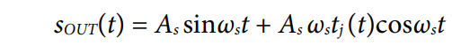
しかし、ADC のサンプリング・クロックの場合は、理想逓倍モデルも非理想逓倍モデルも、クロック・ノイズ・カップリングのメカニズムとそれに伴うジッタを明確に説明することはできません。最も単純なサンプリング・モデルでは、クロックのすべての立上がりエッジが理想サンプリング・インパルスを生成すると仮定します(図 8 参照、クロックおよびサンプリング・パルス列が時間領域と周波数領域の両方で示されていることに注意してください)。このパルス列は、サンプリングされた出力を得るために、入力信号により時間領域で逓倍したものです。入力信号とクロックの間で直接的な逓倍操作はないことに注意してください。したがって、それぞれのスペクトラム間での直接的な畳込みもありません。信号のスペクトラムに畳み込まれるのは、サンプリング・パルス列のスペクトラムですまた、パルス列のスペクトラムは周波数領域のパルス列でもあり、これにより、シャノン-ナイキストのサンプリング定理に示されているような、周知の周期的な出力スペクトラムが得られます。この理論は、サンプリング周波数が十分に高ければ、サンプリングされた出力信号は連続入力信号を正確に表したものになることを証明しています。


ここで、
sOUT(t)は出力信号、
sIN(t)は入力信号、
As は信号振幅、
ωs は信号の角周波数です。
厳密に言うと、この式はサンプリングの時点でのみ成り立ちます。したがって、連続的な時間を表す t ではなく、離散的な時間を表す lTc を使う必要があります。しかし、ほとんどの場合は、表記を簡潔にするために t が使われます。このモデルを使うと、クロック位相ノイズの当然の結果として、ジッタが発生します。
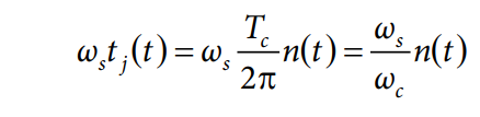
位相ノイズは、サンプリング・パルスを、時間領域でその理想的な位置から移動させます(図 9 参照)。理想クロックからのこのずれは時間間隔誤差(Time Interval Error: TIE)と呼ばれ、tj(t)で表されます。これは適切な数学的モデルを構成しますが、測定は困難です。代わりに、通常は隣接パルス間の時間を測定して、周期ジッタまたはサイクル間ジッタを求めます。TIEは、その後に周期ジッタから計算で求められます。ジッタは、基本的に離散時間の概念であることに注意してください。ジッタは、サンプリング時間においてのみ意味を持ちます。


TIE と位相ノイズの関係は単純です。クロック周期 Tc は、完全な円、つまり 2π の角度に相当します。

修正されたサンプリング・パルス列のスペクトラムは解析的に表現するのが難しいため、出力スペクトラムを表現することもできません。代わりに検討できるのが、ジッタにより発生する瞬時追加誤差です。入力信号は正弦波と仮定します(図 10 参照)。


lTc の代わりに t が使われていますが、これは単に表記を簡潔にするためであることに注意してください。
ωstj(t)<< 1 であるとすると、前述の近似を使うことができます。
ωstj(t)は単純化できることに注意してください。
したがって、以下のような単純な関係が得られます。
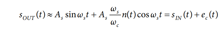
ここで、ec(t)はクロック・ジッタによる追加誤差です。
この結果は、非常に大きな影響をもたらします。近似を行うと、DSB クロックの位相ノイズ n(t)が、入力信号付近に直接マップされます。クロック信号のスペクトラムは入力信号に直接複製されますが、これは相互ミキシングの場合によく似ています。しかしカップリングのメカニズムは異なり、As(ωs/ωc)が定数のために電力も異なります。
この結果は比較も可能にします。次の関係がなり立つ場合は、2つのサンプリング・ソリューションがジッタ・ノイズ電力に関して等しくなります。

逆に、周波数非依存の固定位相ノイズ特性を備えた仮想的な信号発生器をクロックに使用した場合は、その信号発生器を高周波数で使用すると(つまり、より高いレートでサンプリングを行うと)、ジッタ・ノイズ電力が減少します。
アナログ入力
このセクションに至るまで、このアプリケーション・ノートでは、入力信号自体も生成する必要があり、そのプロセスも理想的なものではないので、得られた結果は完全に正確なものではない、という事実を無視してきました。しかし、このようなシステムを説明するためのツールを使用できるようになりました。最初のステップは、入力信号には位相ノイズ m(t)もあるという事実を認識することです。入力とクロックの位相ノイズの間に依存関係はありません。

m(t + tj(t))の部分は、いくつかの仮定によって単純化することができます。信号位相ノイズの形状は周波数領域でピークを形成する可能性が高く、これは非常に広い自己相関関数と同じです。言葉を変えると、任意の時点における信号位相ノイズは、その前の値およびその後の値にごく近い値を示します。さらに tj(t)<< 1 なので、m(t + tj(t))≈ m(t)と仮定することができます。

Asωs⁄ωcn(t)m(t)sinωst 部分はほぼ無視できます。

ここで、es (t)は信号位相ノイズによる追加誤差です。
この場合も、結果は驚くほど単純な関係を示しています。信号位相ノイズを考慮に入れるには、この誤差を単純に追加します。
最後に、この信号の PSD について検討します。各部分の間に相関関係はないので、電力は加算することができます。

ここで、
σOUT(ω)は出力信号の PSD、
σIN(ω)は入力信号の PSD、
εc(ω)はクロック・ジッタによる追加誤差の PSD、
εs(ω)は信号位相ノイズによる追加誤差の PSD です。
展開すると、PSD は次のようになります。

フルスケール基準の結果
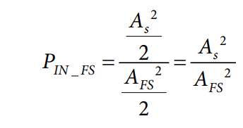
前項に示した説明は数学的には正しいものですが、絶対信号電力 PIN = As2/2 が得られない可能性があるので、実際の状況で使用するのは少し厄介です。信号発生器は、一般的な値に設定することができます。しかし、ADC 入力における実際の信号レベルは、必ずしも分かっていません。損失、減衰、反射、その他の変動要素が、信号が実際に ADC 入力に届くまでの間に、信号に影響を与える可能性があります。したがって、mW で表す絶対的な電力値ではなく、相対的な値が使われます。入力信号電力は、入力におけるフルスケール(FS)信号となる正弦波の電力を基準に表されます。
この場合、PSD は次式のようになります。

信号発生器の DSB 位相ノイズ PSD を示す ν(ω)と μ(ω)は、絶対値ではなく、キャリアに対する相対値で測定されることを思い出してください。すなわち、クロックの公称信号電力と、アナログ入力の公称アナログ入力信号電力です。
最終的に、結果は、負の成分と正の成分の電力を加算するだけで、正の周波数にまとめることができます。

例
ジッタには、確定的なものと確率的なものがあります。このアプリケーション・ノートに示す証明は、できるだけ制約を設けないようにしているので、得られた結果は広い範囲に適用可能で、さまざまなケースにおけるスペクトラム予測に使用することができます。
インターリーブ型 ADC のクロック・スキュー・ジッタ - 複雑な ADC の動作を明確にするための理論を適用
例えば、時間インターリーブ型コンバータでは、複数の同じADC が、個々のコンバータの動作サンプル・レートより高いレートでサンプルを処理します。その結果、配列内の各 ADC が実際に低いレートでサンプリングを行っていても、全体的な正味サンプル・レートは高くなります。したがって、例えば 4 個の 100 MSPS ADC をインターリーブすることによって、原理上は 400 MSPS ADC を実現することができます。
ただし、この概念は、個々の ADC のタイミングの精度が高く、正確であることが前提となります。実際には、1 個の ADCのクロックに他のクロックに対するオフセットが生じている、という状況が発生し得ます。このオフセットは一般にクロック・スキューと呼ばれ、確定的ジッタ、または特有の tj(t)関数を繰返し生成する TIE と見なすことができます。前に示した理論により、最終的に得られるスペクトラムを明確にして予測することができます。位相ノイズは、As(ωs/ωc)として出力信号に直接マップされます。したがって、出力スペクトラムを検討すれば、インターリーブされる ADC のタイミングにオフセットが存在するかどうかを十分に判断することができます。
SMA100A 信号発生器と AD9684 ADC — スペクトラムを予測するための理論を適用
以下の例では、AD9684 高速 ADC の入力クロックとして、ローデ・シュワルツの SMA100A 信号発生器(9 kHz ~ 3 GHz)を使用しました。アナログ入力は、同じタイプの信号発生器によって供給しました。500 MHz で測定した位相ノイズを図 11 に示します。


追加的な入力パラメータ(入力周波数 125 MHz、入力電力レベル −2.0 dBFS、分解能 14 ビット、アパーチャ・ジッタ 80 fs、入力白色ノイズ 1.9 LSB rms、FFT サイズ 131072)を使って、出力スペクトラムを予測できます(図 12 参照)。


このセットアップでの実際の測定データを、図 13 に示します。このケースでは、数学的予測値(薄いグレーのラインで表示)が、実際の測定値と非常によく一致しています。この結果を視野に入れて、AD9684 ADC は、複雑なアナログおよびデジタル信号処理機能を備えたマルチステージのパイプライン・アーキテクチャを採用していますが、その動作は、図 9 に示す単純なモデルと、フルスケール基準の結果のセクションの最後に示す式を使用して、容易に予測することができます。


著者
