
製品概要
製品概要
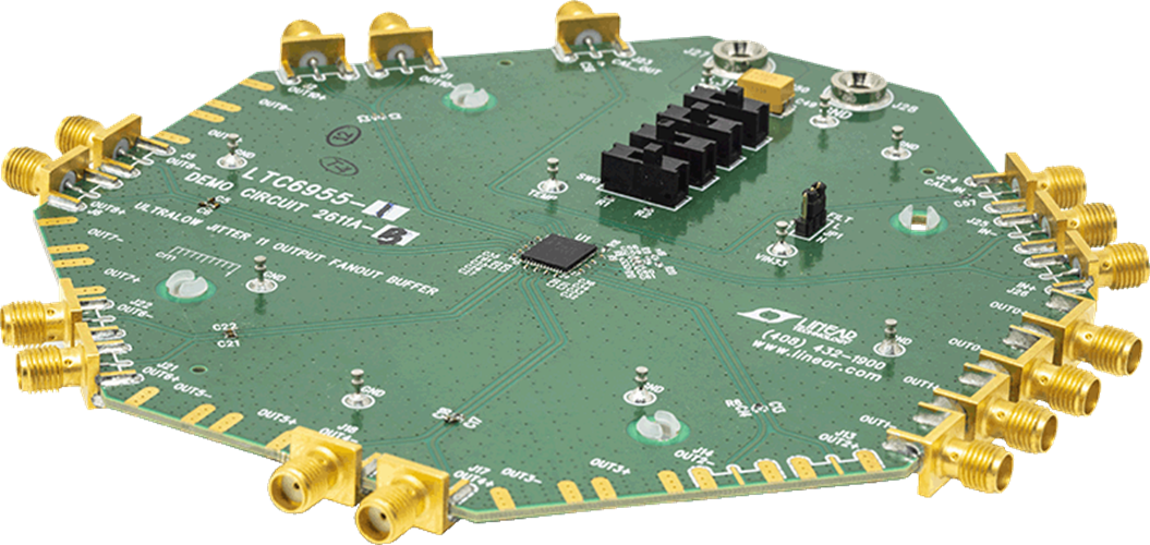
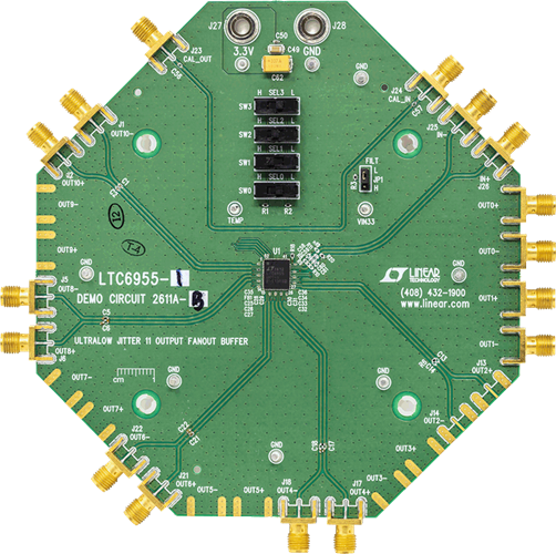
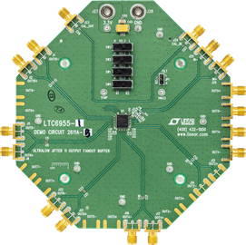
Demonstration Circuit 2611A features the LTC6955-1, Ultralow Jitter 11 Output Fanout Buffers.
By default, the DC2611A is powered from a single 3.3V supply. An option is provided to power to the DC2611A from dual supplies, allowing for the LTC6955-1’s output supply pins to connect to an LTC Silent Switcher® and the LTC6955-1 input supply pin to connect to a low noise LDO.
The differential inputs and six of the differential outputs are populated with 0.5" spaced SMA connectors. These outputs are AC-coupled with 50Ω transmission lines making them suitable to drive 50Ω impedance instruments. All registered trademarks and trademarks are the property of their respective owners.
The remaining four differential outputs are terminated with 100Ω.
A calibration path is provided to aid in accurate LTC6955-1 propagation delay measurements. The calibration path can be also reconfigured as a DC path, which allows for a convenient method of locking the LTC6955-1 outputs to an external PLL/VCO.
関連資料
-
DC2611A - Schematic2018/12/06PDF44 K
-
DC2611A Demo Manual2019/02/20PDF2 M
-
DC2611A - Design Files2018/12/06ZIP4 M